Download
1 / 20
200 likes | 661 Vues
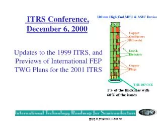
ITRS 2003 Front End Process ITRS Conference December 2, 2003 Hsinchu, Taiwan. Starting Materials: H. Huff, D. Meyers Surface Preparation: J. Butterbaugh, J. Barnett Thermal Films: C. Osburn, H. Huff FEOL Etch: G. Smith, Y. Kim Doping: L. Larson, D. Mercer

E N D
ITRS 2003 Front End ProcessITRS Conference December 2, 2003Hsinchu, Taiwan
Starting Materials: H. Huff, D. Meyers Surface Preparation: J. Butterbaugh, J. Barnett Thermal Films: C. Osburn, H. Huff FEOL Etch: G. Smith, Y. Kim Doping: L. Larson, D. Mercer DRAM Trench Capacitor: Europe FEP, B. Vollmer, M. Gutsche DRAM Stack Capacitor: Japan FEP, M. Kubota, K. Kaneda Flash Memory: M. Alessandri, (Eur)H.K Kang (S. Kor FeRAM: Japan FEP, M. Kubota FEP Technology Working Groups
Introduction of many new materials into the CMOS Logic and DRAM process flows (2003-2007) High k gate dielectric layers Dual metal gates New DRAM storage capacitor structures and materials New substrate materials such as SOI and strained silicon Alternate memory devices and materials, e.g. MRAM, FeRAM Beyond 2007, the probable introduction and CMOS integration of non-standard, dual-gate MOSFET’s e.g. FINFET FEP- The Grand Challenges
2003-2007- Enhanced bulk devices Strained silicon channels Dual work function metal gates (for p-MOS and N-MOS High-k gate dielectric 2008-2011- Planar fully depleted SOI Incorporate bulk enhancements Silicon film thickness ~0.4 Lgate Elevated contacts 2012-2018- Fully Depleted Double Gate MOSFET Scaling- One scenario
Bulk Scaling Challenges- Year 2003-7 2 metals replace dual doped poly High-k replaces Silicon Oxynitride NiSi replaces CoSi2 Strained Si:Ge replaces Si 1/2X every 4-6 years Drain extension Rs problems Metal/Silicon Contact Rs problems Gate Length Scaling and 10% 3 CD Control !!!!!
FD SOI Scaling Challenges 2008-2011 • Challenges: • Dual metal gate integration • CD Control (10% 3) • Spacer integrity • Silicide/Si contact Rs • Active Layer t control • Hi-k integration • Zero Damage Cleaning • Box layer t control • Drain extension Rs and gate drain overlap • Epi-Bulk interface contamination Dual metal gates (nMOS, pMOS) Contact NiSi Sidewall spacer High-k Dielectric Epi Elevated Contact Box Layer Strained Silicon Active Layer Active layer thickness ~0.4 Lgate, must scale with gate length
Double- or Tri-Gate Device Scaling 2011-2018 Silicon Fin Channel Metal Gates 1 & 2 1 2 Source Drain Gate Dielectric Layer (not shown) Buried Oxide Layer = High N doping = Light P doping
FIN FET Challenges • Challenges: • Gate CD Control • Metal Gate Integration • Fin Thickness control • Drain Extension parasitic resistance • Silicon/Silicide contact Resistance • Sidewall spacer integrity • High-k gate dielectric integration • Zero damage cleaning Drain Extensions Gate 1 Drain Source Gate 2 Sidewall Spacers Hi-k Gate Dielectric Layers Fin Thickness ~0.8 Lgate, must scale with gate length scaling
Production Ramp of SOI substrates- Production capacity & capability Metrology capability New Substrate Materials Likely- Strained silicon on bulk Strained silicon on SOI May be a family of products Site Flatness (FEP Difficult Challenge) Difficult to achieve Wafer/chuck interactions add to overall non-flatness Wafer/Chuck interactions poorly understood Starting Materials, Near- Term Issues & Challenges
Near-tem red wall FEP surface cleaning with very low silicon loss FEP surface cleaning with very low silicon oxide loss Cleaning process for newly introduced materials High-k gate dielectric material(s) Dual work function metal gates DRAM High-k capacitor dielectric materials Strained silicon Cleaning of high aspect ratio structures Stacked and Trench capacitors Vias Fragile structures limit cleaning options FEP Surface Preparation
FEP Surface-Preparation, Near-Term Red Wall Note: Loss is defined as the average lost per pass, experienced after multiple cleaning passes: e.g. 0.2 Angstrom loss/pass is equivalent to 2 Angstrom loss after 10 cleaning passes Dry strip and clean processes more complex process flows with more cleans, combined with more shallow structures combine to mandate low substrate loss cleaning processes
10% 3 control of Gate Length represents a significant near term challenge Lithography variances contribute to overall variance Resist & Trim variances also contribute Near Term work-arounds are assume to exist Design for greater variance Accept lesser binning yields Front-End Etch
Etch Challenges Work-arounds exist
Most challenging issue remains the introduction of High-k gate dielectric layers Candidate materials are emerging but none are free of major disadvantages Interface states at channel and at polysilicon gate electrode Poor charge carrier mobility Threshold voltage shifts CMOS integration challenges High-k gate dielectric layers require introduction before 2007 for low standby power MOSFETS Lowered gate leakage allowance (vs 2001 ITRS) for HP drives need High-k gate dielectric in 2007 Gate leakage for Low Standby Power Devices drives need for high-k gate dielectric in 2006 Gate Dielectric Layer Thickness control is emerging as an important challenge STI added for 2003 Roadmap FEP Thermal/Films
Major challenges continue to surround the achievement of ultra-shallow, abrupt, highly activated drain extensions. Drives innovation in ion implantation processes & equipments Drives R&D for very rapid activation processes Attempts at more sophisticated model-based forecasting of Source/Drain requirements have not yet yielded conclusive results S/D requirements highly interactive with overall transistor design S/D requirements for bulk devices are different from SOI and future non-planar double gate devices Drain Extension requirements are listed as target values Modeling of polysilicon gate depletion suggest that metal gates have potential to significantly extend the life of SiON gate dielectric materials FEP/Doping
HP Logic, Metal Gate Delays Need for High-k Gate Dielectric Modeling done by H. Gossmann, Axcelis Technologies Inc.
Chip Size Model modified, based on survey of DRAM manufacturers Storage cell area increased from prior ITRS DRAM peripheral area decreased from prior ITRS Need for very high-k storage capacitor dielectric materials (e.g. BST) delayed beyond 2009 Aluminum Oxide, Aluminates (e.g. HfAlOx) and Tantalum oxide remain capacitor materials of consideration for the 2003-9 time period Capacitor structure migrates from MIS to MIM in order to avoid challenges regarding capacitor dielectric thickness Total interlevel metal +dielectric (except storage node) is assumed to be 1.08nm at the 180nm node, and to decrease at a rate of 10% every three years. Storage node heights, dielectric constants of high-k materials, and capacitor structures (cylinder, etc) remain unchanged from prior roadmaps DRAM Stacked Capacitor