Derandomiser block
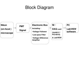
This article outlines the core structure and layout of a derandomizer chip, along with expected specifications and analog readout architecture. It discusses the prototype design, output and input channels, crosspoint switch, arbitration logic, and storage devices.

Derandomiser block
E N D
Presentation Transcript
Derandomiser block E.Atkin, A.Kluev MEPhI, A.Voronin SINP MSU
Outline • Core structure of derandomiser • Specs expected • Chip structure and layout
Analog readout architecture with derandomizer Prototype Output channel 0 Input channel 0 PD ADC CSA Shaper Analog output 0 CMP Digital input 0 Analog input 0 Address bus 0 Crosspoint switch + Arbitration logic: n inputs, m outputs n>m busy Output channel m PD ADC Analog output m Analog input n Input channel n CSA Shaper CMP Digital input n Address bus m busy
Crosspoint switch architectures Multiple storages shared by channels Analog storage devices (T&H or PD) Crosspoint switch ADCs ● ● ● Address IN1 IN2 ● ● ● ● ● ● INn Arbitration Preamps + Shapers Comparators
First prototype 4 x 2 X0, X1, X2, X3 – analog inputs, Y0, Y1 – cross-point switch outputs
What were simplified on the first prototype • We do not think about cross talk, linearity, noise • There are no drivers on the chip outputs • Idea was to check derandomizer fuctionality • We did not check the arbitration logic for infinity, when input signals have small delays or no delay • Peak detector is not optimized for HOLD mode • Cross-point switch is not optimized for capacitive load
Comparator 1 2 2 1us 1 1us 1 1us 2 3 3 3 Cload =1 pF 2 1 2 3 1us 1 3 2 Cload =1 pF 1us 3 1 2 Cload =4 pF 1 • Colored – simulation • B/W – scope • 1 – input • 2 –output • 3 – threshold level 3 2 Cload =15 pF Cload =15 pF
Peak Detector 2.5us 2.5us 2.5us 3 3 3 2 1 1 2 2 1 Cload =15 pF Cload =1 pF Cload =4 pF 3 3 2 1 1 1 2 2 Cload =15 pF Cload =15 pF Cload =15 pF • Colored – simulation • B/W – scope • 1 – input • 2 –output • 3 – reset
Cross point switch 2 1 1 1 3 3 Only one signal on the input Two signals on different time • 1 - comparators • 2 – inputs • 3 – outputs
Cross point switch 1 1 2 2 Small delay between two signals Two signals in the same time • 1 - comparators • 2 – inputs • 3 – outputs
Cross point switch 4 Signals (4 comparators) 2 cross-point switch outputs (with amplification)
Cross point switch 4 Signals ( 4 comparators) 2 cross-point switch outputs and peak detectors
Comments • The prototype chip confirmed derandomizer functionality • Schematics should be improved for signals, which can come in the same time (to avoid infinity on the cross-point switch outputs) • Next prototype must get much less cross talk between channels and different parts of the chips • To measure the real speed of the scheme the fast drivers should be included on the chip outputs • Service low capacitance outputs better to measure with picoprobe, which is serious problem for us