Download
1 / 22
220 likes | 424 Vues
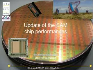
Update of the SAM chip performances eric.delagnes@cea.fr breton@lal.in2p3.fr. Séminaire DRT/LIST 08/09/08 SACLAY. Saclay’s experience on SCAs: > 100k channels working worldwide. AFTER : 05-06 TPC of T2K 72 ch/ 512 pts Fe= 1-50 Mhz,BP = 10 Mhz Dyn= 10 bits AMS0.35 µm. Also includes FE.

E N D
Update of the SAMchip performanceseric.delagnes@cea.frbreton@lal.in2p3.fr Séminaire DRT/LIST 08/09/08 SACLAY.
Saclay’s experience on SCAs: > 100k channels working worldwide AFTER : 05-06 TPC of T2K 72 ch/ 512 pts Fe= 1-50 Mhz,BP = 10 Mhz Dyn= 10 bits AMS0.35 µm. Also includes FE. 500k transitors New Architectures ARS0 : 97-98 ANTARES/HESS1 5 ch/ 128 pts Fe= 1Gs/S BP = 80 Mhz Dyn~8-9bits AMS 0.8 µm KM3Net ARS1 : 98-04 ANTARES 4 Ch system on chip including ARS0 CTA HAMAC : 93-97 Calo ATLAS 12 canaux/ 144 pts Fe= 40 Mhz BP = 10 Mhz Dyn= 13,6 bits DMILL 0.8 µm SAM 04-05 HESS2 2 ch / 256 pts Fe= [50 MHz-2GHz] BP = 300 Mhz Dyn= 12 bits AMS 0.35 µm MATACQ : 99-01 Matrix Structure 1 ch, 2560 pts Fe= 50 MHz-2GHz BP = 300 Mhz Dyn= 12 bits AMS 0.8 µm (PATENT) FastSampler Fs~ 5-10GHz , BW>600MHz >5000 pts ? DSM technology +LAL PIPELINE :01- 02 METRIX 1 ch System on chip integrating 1 MATACQ Continuous Sampler 1 GS/s- 12 bit PATENT design 2008 Future
The ARS0 chip: first GS/s sampler designed @ Saclay • Gsample/s time expander chip originally developed for the ANTARES experiment based in the Mediterranean Sea. • Based on sampling-DLL technique : • 5 channels /chip, 128 cells per channel. • Circular buffer • Sampling @ 1 GHz • Limited to 80 MHz BW because of input buffers • Readout ~ 1 MHz/sample triggered by an external signal • A programmable number of cells is read starting from a programmable offset from the trigger • Low power (500mW). • 8-9 bits dynamic range AMS CMOS 0.8µm Heart of the ARS1 chip for ANTARES Used @ CEBAF by IN2P3/LPC Used by HESS I 5000 chips in use
The SAM (swift analog memory) chip for the HESS2 experiment • Same functionalities than ARS0 but with higher performances: • High RO speed Gsample/s time expander chip. • Required to treat the extended dynamic of the new telescope Number of ch 2 differential Number of cells/ch 256 BW > 250 MHz Sampling Freq 700MHz-2.5GHz High Readout Speed >16 MHz Simultaneous R/W No Smart Read pointer Yes (integrate a 1/Fs step TDC) Few external signals (<> from MATACQ). Many modes configurable by a serial link. Auto-configuration @ power on Low cost for medium size prod=> AMS 0.35 µm 6000 ASICs manufactured,tested and delivered in Q2 2007 NIM A, Volume 567, Issue 1, p. 21-26, 2006
Principle of the SAMPLING MATRIX 1 ampli/line short DLL: less jitter Parallelized Readout 1 delay servo-control /col: stability
Advantages/ Drawbacks of the Sampling MATRIX structure • Short DLL: • smaller jitter. • junction between DLLs. • potential coupling between Analog Signal and DLL control voltage. • 1 servo control of Delay / Col: => high stability. • Analog Input Buffering: • High input impedance: • Linearity. • No DC input current • No Ringing. Flat response • Power consumption. • BW limitation • Analog Bus Split in divisions : lines • shorter analog bus : • More uniform bandwidth. • less analog delay along the bus. • Parallel readout => faster readout. • 1 buffer / line : • Better analog BW/power consumption FOM. • Spread of the buffer bandwidth. • Offset between lines (corrected by DAC on-chip). • Initial Philosophy: No Off-chip correction (pedestal, amplitude, time)=> limit external computing.
Fixed Pattern Apperture Jitter • Device Mismatches of components in the delay chain : • => spread of delay duration. • => error on the sampling time. • => fixed for a given tap => fixed pattern apperture jitter • spread of single delays => time DNL. • cumulative effect => time INL. • systematic effect => possible correction if cell index is known • Drawbacks: computing power + non equidistant samples (FFT). • => Good calibration required.
Jitter vs DLL length • 2 sources of aperture jitter : • Random aperture jitter (RAJ). • Fixed Pattern Aperture Jitter (FPJ). • Inside the DLL, jitters are cumulative. Assuming there is no correlation: • For RAJ, the aperture jitter @ tap j will be • if sRd is the random jitter added by a delay tap • For FPJ • for a free running system • if the total delay is servo-controlled • if sFPdis the random jitter added by a delay tap (sDNL) and N is the DL length. • Short DL => Less Jitter (both kinds)
Variable BW along the SCA. Analog in • Analog Bus is a RC delay line: • Delay depends on the sampling cell position. • The overall Bandwidth also does, especially if it is not limited by an input amplifier or that of the intrinsic sampling cell. Short analog busses are better for BW uniformity => segmentation
New Results On the SAM chip. • SAM designed for HESS-2 experiment: • low cost in medium volume (11mm2/AMS 0.35) • memory depth made to match the trigger latency (256 cells) • BW required ~ 250MHz. • Fsample: 1GS/s -> 2GS/s. • Characterized on a test bench based on the HESS-2 FEC with limited capabilities • New test bench = USB 2 powered board designed @ LAL, permits • understanding the real limits of the chip before starting the design for CTA. • the evaluation for fast timing application (demonstrator for reflectometry) performances as published in the NIM paper
The SAM-USB board (received Sept 3rd 2008) Power consumption < 2.5W Reference Clock. Up to 200MHz=> 3.2GS/s pulser for reflectometry applications 1 GHz BW amplifier. 2 analog inputs. DC coupled µ USB Ext clk & Trigger inputs Dual 12 bit ADC SAM Chip Trigger discriminators
New Results • Input Dynamic range can go up to 4V differential • 12.6 bits dynamic range. • Max Sampling Frequency > 3.2 GS/s • 450 MHz -3dB BW (for a full range signal): • ~800 MHz roll off point • convolution of SAM + on-board 1GHz amplifier. • no ringing.
New Results: Crosstlak vs frequency Xtalk < 1% even for high frequencies
New Results: Short pulse sampling 1ns FWHM pulse sampled @ 3.2GS/s (75mV) single shot
New Results: Reflectometer mode • Original target application of the board. • 2 mm precision reached (in repetitive mode). single shot
Timing resolution . • First, without any correction • 2 methods used for global resolution measurement: • measurement of ENOB on sinewaves. • measurement with pulses.
ENOB measurement. • ENOB is not Log( Max signal/noise)/ Log(2) as often said. • ENOB = (10 Log (sinus power / residues power) -1.76)/6.02. • Depends on input sinewave frequency, noise & jitter. • Contribution of jitter to ENOB = (20 Log (2.Pi .s .Fsine))-1.76)/6.02. smeas consistent with 25ps rms 197 MHz sinewave/ 3.2GS/s
Timing measurement with pulses. • asynchronous pulse with fixed amplitude summed with same delayed reflected (by cable) pulse . • time difference between the two pulses extracted by fixed threshold crossing (determined by simple linear interpolation). • sdelay = 35ps rms =>25ps for each pulse • Consistent with ENOB measurement. • Pulse timing can be improved by using more than 2 samples => To Be Done
Extraction of fixed pattern and random jitter. • Method: • 197MHz sinewave sampled by SAM • Search of zero-crossing segment => length and position (cell). • Histogram of length[position]: • propor. to time step duration (assuming sine = straight line). • small bias due to sinewave curvature (<1.7ps rms/ 197MHz sine) • mean_length[position] = fixed pattern effect • sigma_length[position] = random effect
Fixed pattern jitter • DNL => modulo 16 pattern. Time step spread = 6.6 ps rms • INL => modulo 16 pattern + slow pattern. • “Absolute time” spread = 23 ps rms (100 ps peak-peak) • Seems to be the major part of the jitter. • Position correlated => could be corrected (off-chip) => TO BE DONE
Random jitter with random trigger with trigger on sinewave • With random trigger : jitter floor ~ 2ps rms but with large jitter on “transition” samples (32 ps). Mean jitter ~ 5 ps • If trigger on sinewave => jitter peak decreases to 5ps. Mean jitter ~ 2.5 ps rms • “Nearly” understood (coupling between analog signal and DLL command). • Will be corrected on future chips/boards. Might even be suppressed on this one.
Conclusion • The new USB board allowed to push the SAM chip towards its limits. • Timing measurements show a timing resolution of ~25 ps rms without any off-chip correction. • Timing resolution with correction and using several samples under study. • Very small random jitter (few ps). • Some work still has to be done to optimize the board performances. • Tests have already given us new guidelines for future chips to improve timing performances. • Next circuit will be submitted beginning 2009: same sampling frequency, same technology, larger depth => target = CTA experiment • We are now convinced that a single chip can hardly be optimum for all applications (depth vs time precision). • Upgraded version of the SAM-USB board will soon be available. • Can be used for low cost fast detector testing. • Will be compatible with the next generation chips • Will be available in a small plastic case