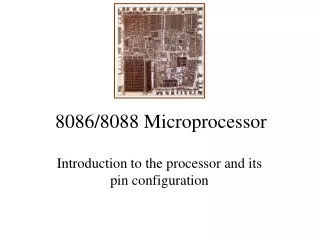
The 8088 and 8086 Microprocessors
The 8088 and 8086 Microprocessors. The 8086, announced in 1978, was the first 16-bit microprocessor introduced by Intel Corporation 8086 and 8088 are internally 16-bit MPU. Externally the 8086 has a 16-bit data bus and the 8088 has an 8-bit data bus. The 8088 and 8086 Microprocessors (cont.).

The 8088 and 8086 Microprocessors
E N D
Presentation Transcript
The 8088 and 8086 Microprocessors • The 8086, announced in 1978, was the first 16-bitmicroprocessor introduced by Intel Corporation • 8086 and 8088 are internally 16-bit MPU. • Externally the 8086 has a 16-bit data bus and the8088 has an 8-bit data bus
The 8088 and 8086 Microprocessors (cont.) • 8086 and 8088 both have the ability to address up to 1 Mbyte of memory and 64K of input/output port • The 8088 and 8086 are both manufactured using high-performance metal-oxide semiconductor (HMOS) technology • The 8088 and 8086 are housed in a 40-pin dual inline package and many pins have multiple functions
The 8088 and 8086 Microprocessors (cont.) • CMOS, Complementary Metal-Oxide-Semiconductor, is a major class of integrated circuits used in chips such as microprocessors, microcontrollers, static RAM, digital logic circuits, and analog circuits such as image sensors • Two important characteristics of CMOS devices are high noise immunity and low static power supply drain. • Significant power is only drawn when its transistors are switching between on and off states
The 8088 and 8086 Microprocessors (cont.) CMOS devices do not produce as much heat as other forms of logic such as TTL. CMOS also allows a high density of logic functions on a chip
The 8088 and 8086 Microprocessors (cont.) Pin layout of the 8086 and 8088 microprocessor
8086 Features • 16-bit Arithmetic Logic Unit • 16-bit data bus (8088 has 8-bit data bus) • 20-bit address bus - 220 = 1,048,576 = 1 meg The address refers to a byte in memory. In the 8088, these bytes come in on the 8-bit data bus. In the 8086, bytes at even addresses come in on the low half of the data bus (bits 0-7) and bytes at odd addresses come in on the upper half of the data bus (bits 8-15). The 8086 can read a 16-bit word at an even address in one operation and at an odd address in two operations. The 8088 needs two operations in either case. The least significant byte of a word on an 8086 family microprocessor is at the lower address.
8086 Architecture • • The 8086 has two parts, the Bus Interface Unit (BIU) and the • Execution Unit (EU). • • The BIU fetches instructions, reads and writes data, and computes the • 20-bit address. • • The EU decodes and executes the instructions using the 16-bit ALU. • • The BIU contains the following registers: • IP - the Instruction Pointer • CS - the Code Segment Register • DS - the Data Segment Register • SS - the Stack Segment Register • ES - the Extra Segment Register • The BIU fetches instructions using the CS and IP, written CS:IP, to contract • the 20-bit address. Data is fetched using a segment register (usually the DS) • and an effective address (EA) computed by the EU depending on the • addressing mode.
The EU contains the following 16-bit registers: • AX - the Accumulator • BX - the Base Register • CX - the Count Register • DX - the Data Register • SP - the Stack Pointer \defaults to stack segment • BP - the Base Pointer / • SI - the Source Index Register • DI - the Destination Register • These are referred to as general-purpose registers, although, as seen by • their names, they often have a special-purpose use for some instructions. • The AX, BX, CX, and DX registers can be considers as two 8-bit registers, a • High byte and a Low byte. This allows byte operations and compatibility with • the previous generation of 8-bit processors, the 8080 and 8085. 8085 source • code could be translated in 8086 code and assembled. The 8-bit registers are: • AX --> AH,AL • BX --> BH,BL • CX --> CH,CL • DX --> DH,DL
8086 Programmer’s Model ES Extra Segment BIU registers (20 bit adder) CS Code Segment SS Stack Segment DS Data Segment IP Instruction Pointer EU registers AX AH AL Accumulator BX BH BL Base Register CX CH CL Count Register DH DL DX Data Register SP Stack Pointer BP Base Pointer Source Index Register SI DI Destination Index Register FLAGS
8086/88 internal registers 16 bits (2 bytes each) AX, BX, CX and DX are two bytes wide and each byte can be accessed separately These registers are used as memory pointers. Flags will be discussed later Segment registers are used as base address for a segment in the 1 M byte of memory
The 8086/8088 Microprocessors: Registers • Registers • Registers are in the CPU and are referred to by specific names • Data registers • Hold data for an operation to be performed • There are 4 data registers (AX, BX, CX, DX) • Address registers • Hold the address of an instruction or data element • Segment registers (CS, DS, ES, SS) • Pointer registers (SP, BP, IP) • Index registers (SI, DI) • Status register • Keeps the current status of the processor • On an IBM PC the status register is called the FLAGS register • In total there are fourteen 16-bit registers in an 8086/8088
Data Registers: AX, BX, CX, DX • Instructions execute faster if the data is in a register • AX, BX, CX, DX are the data registers • Low and High bytes of the data registers can be accessed separately • AH, BH, CH, DH are the high bytes • AL, BL, CL, and DL are the low bytes • Data Registers are general purpose registers but they also perform special functions • AX • Accumulator Register • Preferred register to use in arithmetic, logic and data transfer instructions because it generates the shortest Machine Language Code • Must be used in multiplication and division operations • Must also be used in I/O operations
BX • Base Register • Also serves as an address register • Used in array operations • Used in Table Lookup operations (XLAT) • CX • Count register • Used as a loop counter • Used in shift and rotate operations • DX • Data register • Used in multiplication and division • Also used in I/O operations
Pointer and Index Registers • Contain the offset addresses of memory locations • Can also be used in arithmetic and other operations • SP: Stack pointer • Used with SS to access the stack segment • BP: Base Pointer • Primarily used to access data on the stack • Can be used to access data in other segments • SI: Source Index register • is required for some string operations • When string operations are performed, the SI register points to memory locations in the data segment which is addressed by the DS register. Thus, SI is associated with the DS in string operations.
DI: Destination Index register • is also required for some string operations. • When string operations are performed, the DI register points to memory locations in the data segment which is addressed by the ES register. Thus, DI is associated with the ES in string operations. • The SI and the DI registers may also be used to access data stored in arrays
Segment Registers - CS, DS, SS and ES • Are Address registers • Store the memory addresses of instructions and data • Memory Organization • Each byte in memory has a 20 bit address starting with 0 to 220-1 or 1 meg of addressable memory • Addresses are expressed as 5 hex digits from 00000 - FFFFF • Problem: But 20 bit addresses are TOO BIG to fit in 16 bit registers! • Solution: Memory Segment • Block of 64K (65,536) consecutive memory bytes • A segment number is a 16 bit number • Segment numbers range from 0000 to FFFF • Within a segment, a particular memory location is specified with an offset • An offset also ranges from 0000 to FFFF
Segmented Memory Segmented memory addressing: absolute (linear) address is a combination of a 16-bit segment value added to a 16-bit offset one segment linear addresses
Offset Value (16 bits) 0 0 0 0 Segment Register (16 bits) Adder Physical Address (20 Bits) Memory Address Generation Intel • The BIU has a dedicated adder for determining physical memory addresses
2 9 Offset: 0 0 0 0 0 0 0 0 0 0 1 0 1 0 0 1 Segment: 0 0 0 1 0 0 0 0 0 0 0 0 0 0 0 0 0 0 0 0 Address: 0 0 0 1 0 0 0 0 0 0 0 0 0 0 1 0 1 0 0 1 Example Address Calculation Intel • If the data segment starts at location 1000h and a data reference contains the address 29h where is the actual data?
Segment:Offset Address • Logical Address is specified as segment:offset • Physical address is obtained by shifting the segment address 4 bits to the left and adding the offset address • Thus the physical address of the logical address A4FB:4872 is • A4FB0 • + 4872 • A9822
Your turn . . . What linear address corresponds to the segment/offset address 028F:0030? 028F0 + 0030 = 02920 Always use hexadecimal notation for addresses.
Your turn . . . What segment addresses correspond to the linear address 28F30h? Many different segment-offset addresses can produce the linear address 28F30h. For example: 28F0:0030, 28F3:0000, 28B0:0430, . . .
The Code Segment 0H 4000H CS: 0400H 4056H IP 0056H CS:IP = 400:56 Logical Address Memory 0400 0 Segment Register Offset Physical or Absolute Address + 0056 0FFFFFH 04056H The offset is the distance in bytes from the start of the segment. The offset is given by the IP for the Code Segment. Instructions are always fetched with using the CS register. The physical address is also called the absolute address.
The Data Segment 0H 05C00H 05C0 DS: 05C50H 0050 EA DS:EA Memory 05C0 0 Segment Register Offset Physical Address + 0050 0FFFFFH 05C50H Data is usually fetched with respect to the DS register. The effective address (EA) is the offset. The EA depends on the addressing mode.
The Stack Segment 0H 0A000H 0A00 SS: 0A100H SP 0100 SS:SP Memory 0A00 0 Segment Register Offset Physical Address + 0100 0FFFFFH 0A100H The offset is given by the SP register. The stack is always referenced with respect to the stack segment register. The stack grows toward decreasing memory locations. The SP points to the last or top item on the stack. PUSH - pre-decrement the SP POP - post-increment the SP
Flags Carry flag Overflow Parity flag Direction Interrupt enable Auxiliary flag Trap Zero Sign 6 are status flags 3 are control flag
Flag Register • Conditional flags: • They are set according to some results of arithmetic operation. You do not need to alter the value yourself. • Control flags: • Used to control some operations of the MPU. These flags are to be set by you in order to achieve some specific purposes. • CF (carry) Contains carry from leftmost bit following arithmetic, also contains last bit from a shift or rotate operation.
Flag Register • OF (overflow) Indicates overflow of the leftmost bit during arithmetic. • DF (direction) Indicates left or right for moving or comparing string data. • IF (interrupt) Indicates whether external interrupts are being processed or ignored. • TF (trap) Permits operation of the processor in single step mode.
SF (sign) Contains the resulting sign of an arithmetic operation (1=negative) • ZF (zero) Indicates when the result of arithmetic or a comparison is zero. (1=yes) • AF (auxiliary carry) Contains carry out of bit 3 into bit 4 for specialized arithmetic. • PF (parity) Indicates the number of 1 bits that result from an operation.
Minimum-Mode and Maximum-Mode System (cont.) Signals common to both minimum and maximum mode
Minimum-Mode and Maximum-Mode System (cont.) Unique minimum-mode signals
Minimum-Mode and Maximum-Mode System (cont.) Unique maximum-mode signals
Minimum-Mode Interface Block diagram of the minimum-mode 8088 MPU
Minimum-Mode Interface (cont.) Block diagram of the minimum-mode 8086 MPU
Minimum-Mode Interface (cont.) • The minimum-mode signals can be divided into the following basic groups: • Address/Data bus • Status signals • Control signals • Interrupt signals • DMA interface signals
Minimum-Mode Interface (cont.) • Address/Data bus • The address bus is used to carry address information to the memory and I/O ports • The address bus is 20-bit long and consists of signal lines A0 through A19 • A 20-bit address gives the 8088 a 1 Mbyte memory address space • Only address line A0 through A15 are used when addressing I/O. • This give an I/O address space of 64 Kbytes • The 8088 has 8 multiplexed address/data bus lines (A0~A7) • 8086 has 16 multiplexed address/data bus lines (A0~A15)
Minimum-Mode Interface (cont.) • Status signals • The four most significant address, A19 through A16 are multiplexed with status signal S6 through S3 • Bits S4 and S3 together form a 2-bit binary code that identifies which of the internal segment registers was used to generate the physical address. • S5 is the logic level of the internal interrupt flag. • S6 is always at the 0 logic level
Maximum-Mode Interface • The maximum-mode configuration is mainly used for implementing a multiprocessor/coprocessor system environment • Multiple processors exist in the system • Each executes its own program • Global resources and local resources • The former are common to all processors • The latter are assigned to specific processors • In the maximum-mode, facilities are provided for implementing allocation of global resources and passing bus control to other microprocessors sharing the system bus