Download
1 / 38
380 likes | 518 Vues
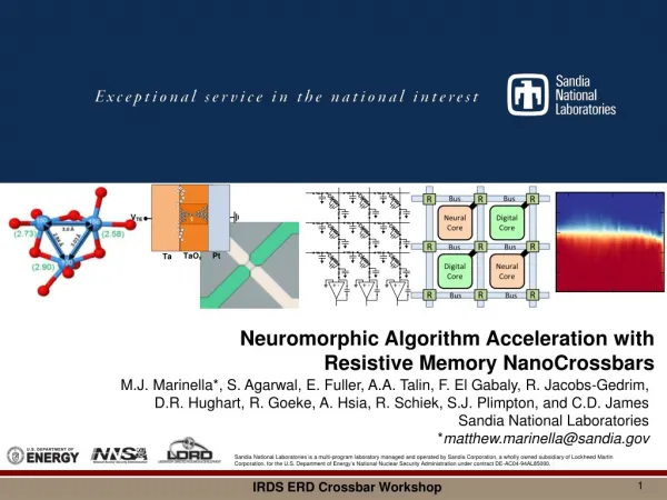
Neuromorphic Algorithm Acceleration with Resistive Memory NanoCrossbars. M.J . Marinella*, S. Agarwal , E. Fuller, A.A . Talin , F. El Gabaly, R. Jacobs-Gedrim, D.R. Hughart, R. Goeke , A. Hsia, R. Schiek , S.J. Plimpton, and C.D . James Sandia National Laboratories

E N D
Neuromorphic Algorithm Acceleration with Resistive Memory NanoCrossbars M.J. Marinella*, S. Agarwal, E. Fuller, A.A. Talin, F. El Gabaly, R. Jacobs-Gedrim, D.R. Hughart, R. Goeke, A. Hsia, R. Schiek, S.J. Plimpton, and C.D. James Sandia National Laboratories *matthew.marinella@sandia.gov 1
Outline Intro and Key Concepts Device Requirements for a Crossbar Accelerator Modeling ReRAM in a Crossbar Accelerator CoDesignFramework Concept Conclusion
Why do we need more efficient computers? Q. Le, IEEE ICASSP 2013 • Google Deep Learning Study • 16000 core, 1000 machine GPU cluster • Trained on 10 million 200x200 pixel images • Training required 3 days • Training set size set by what can be completed in less than one week • What would they like to do? • ~2 billion photos uploaded to internet per day (2014) • Can we train a deep net on one day of image data? • Assume 1000x1000 nominal image size, linear scaling (both assumptions are unrealistically optimistic) • Requires 5 ZettaIPSto train in 3 days (ZettaIPS=1021IPS; ~5 billion modern GPU cores) • Data is increasing exponentially with time • Need >1016-1018 instruction-per-second on 1 IC • Less than 10 fJ per instruction energy budget
Where Are we Today? • Single Unit: Nvidea Tesla P100 GPU • Most advanced GPU processor specs (announced, not yet released) • Target’s deep learning and neural applications • 20 TFLOP/s 16 bit peak performance w/ peak power dissipation of 300W • 70 GFLOP/watt or about 15 pJ/FLOP (16 bit) • Supercomputer: Sunway TaihuLight(China) • Top supercomputer in the world • ShenWei processor • 90 PFLOP/s peak, 15 MW power • 6 GFLOP/W or about 170 pJ/FLOP • Need >1000x improvement
Evolution of Computing Machinery 105pJ/MAC 1980’s Improvements Due Soley to Transistors (Moore’s Law and Denard Voltage Scaling) Early DSP Demonstrations 1990’s 104pJ/MAC 2000’s 103pJ/MAC Modern GPU, 32 bit precision 2010-Present 102pJ/MAC Single GPU Card, Late 2016 10 pJ/MAC ExascaleSystem Goal 2025? 1 pJ/MAC 1 TMAC/W Analog VMM Prototypes 100 fJ/MAC 10 fJ/MAC “Let physics do the computation” Our brain is the ultimate example of this paradigm 2035? 1 fJ/MAC Neuromorphic Target (Efficiency only possible with neural hardware & algorithms) 100 aJ/MAC 10 aJ/MAC Modified from Hasler and Marr, Frontiers in Neuroscience, 2013 1 aJ/MAC Biological Neurons* *Caveat: Biological neurons probably do not perform MACs 5
Resistive RAM (ReRAM) Read Window Highest current switching process • ERD: Bipolar Metal Oxide Redox RAM • Resistance is modulated in a metal oxide • Scalable to 5nm, sub pJ switching energies • TiN/Ta/TaOx/TiN used as example material (SNL version) • CrossSimmodeling applies to all resistive switching crossbars • We will demonstrate simulation of other novel devices also
Crossbar Theoretical Limits • Potential for 100 Tbit of ReRAM on chip • If each can perform 1M computations of interest per second (1 M-op): • 1012 active devices/chip x 106 cycle per second 1018compsper second per chip • Exascale-computations per sec on one chip! • In order to not melt the chip, entire area must be limited to ~100W • Allowed energy per operation = P x t/op = 100W / 1018 = 10-16 = 100 aJ/operation • 10nm line capacitance = 10 aF • Can charge line to 1V with 10 aJ • Drawback: “only” ~100B transistors/chip
How does a crossbar perform a useful computation per device? Mathematical Electrical V W VTW=I V1 W1,1 W1,2 W1,3 V1 V2 V3 G1,1 G1,2 G1,3 = V2 W2,1 W2,2 W2,3 G2,1 G2,2 G2,3 V3 W3,1 W3,2 W3,3 G3,1 G3,2 G3,3 I1=ΣVi,1Wi,1 I2=ΣVi,2Wi,2 I3=ΣVi,3Wi,3 I I1=ΣVi,1Gi,1 I2=ΣVi,2Gi,2 I3=ΣVi,3Gi,3 Electronic Vector Matrix Multiply
Why is it essential to cram so many computations on a single chip? Can you simply connect millions of ultra-efficient chips? Yes, but every time data leaves the chip, it is elevated in the comm hierarchy Energy efficiency per operation is reduced Crossbar accelerator cores
Outline Intro and Key Concepts Device Requirements for a Crossbar Accelerator Modeling ReRAM in a Crossbar Accelerator CoDesignFramework Concept Conclusion
Mapping Backprop to a Crossbar Output Neuron Backpropagated error from following layer w… w1 w2 ctrl 1 ctrl 2 Inputs Error Sum Error Sum Error Sum Backpropagated error to previous layer Inputs from previous layer out in ctrl 1 Vector Matrix Multiply, Rank 1 Update: Key kernel used in many algorithms Outputs to next layer Neuron Neuron Neuron
Experimental Device Nonidealities Read Noise I0+∆I IGW I0 I0-∆I Time (Vread=100mV) Conductance versus Pulse = Ideal = Write Variability = Nonlinear Symmetric and Linear GW Asymmetric, Nonlinear Pulse Number (Vwrite=1V, tpulse=1µs) Ideally weight would increase and decrease linearly Experimental devices have several Device: Write Variability, Write Nonlinearity, Asymmetry, Read Noise Circuit: A/D, D/A noise, parasitics
CrossSim Training and Classification with Read Noise • No read noise present Classification w/ read noise: minimal accuracy degradation until σRN≈0.05 Training w/ read noise: minimal accuracy degradation until σRN≈0.05
CrossSim Training with Write Noise σWN=0 σWN=0 σWN=0 Classification with write noise: Much more sensitive to noise Depends on dataset and initial weigh choice
Device Requirements • Conclusions: • Read noise within typical device capabilities, • Write noise requirement very difficult to meet • Low current requirement provides additional challenge • Next: Measure and assess experimental resistive switches against these requirements 15
Outline Intro and Key Concepts Device Requirements for a Crossbar Accelerator Modeling ReRAM in a Crossbar Accelerator CoDesignFramework Concept Conclusion
TaOx ReRAM Model Delta G vs G (Decreasing Conductance) G versus Pulse Number (V=-1V, pulse width = 50ns) CDF Modeling effect of bipolar TiN/Ta/TaOx/TiNReRAM Pulse through all states repeatedly Arrange data as required by CrossSim model Create look-up table and analytical noise model for higher-level numerical simulation
TaOx ReRAM in BackpropTraning Increasing Network Size Strong dependence on data set and network size
Li-Ion Synaptic Transistor for Analog Computation (LISTA) G-V for LISTA Transistor
Analog State Characterization TaOx ReRAM LISTA > 200 states PCM Array GW Burr et al, IEEE TED 2015
LISTA-device Performance for Backprop Algorithm Increasing Network Size
Next Steps • CrossSim/Xyce circuit-level crossbar energy analysis • Can model fundamental limits and current devices • Select device model is implement • Explore circuit techniques to improve algorithm performance (w/ less than perfect devices) • Design accelerator microarchitecture • Routing technique tradeoffs and comm hierarchy • Local computation capabilities • Local cache sizes (SRAM bits per crossbar bit) • Model system energy and performance
Outline Intro and Key Concepts Device Requirements for a Crossbar Accelerator Modeling ReRAM in a Crossbar Accelerator CoDesignFramework Concept Conclusion
DOE Vision: Universal Multiscale CoDesign Framework 10,000x improvement: 10 fJ per instruction equivalent Application Performance Modeling Modeling Systems • Computer System Architecture Modeling • Next generation of Structural Simulation Toolkit • Heterogeneous systems HPC models • Component Fabrication • Processors, ASICs • Photonics • Memory • Component Level Models • Gem5, McPAT, HiHAT, CACTI, NVSIM • Test Circuit Fab and Measurement • Subcircuit measurement • Circuit/IP Block Design and Modeling • SPICE/Xyce model Devices • Device Measurements • Single device electrical behavior • Parametric variability • Compact Device Models • Single device electrical models • Variability and corner models TEM/EELS • Device Physics Modeling • Device physics modeling (TCAD) • Electron transport, ion transport • Magnetic properties • Device Structure Integration and Demonstration • Novel device structure demonstration Materials • Process Module Modeling • Diffusion, etch, implant simulation • EUV and novel lithography models • Process Module Demonstrations • EUV and novel lithography • Diffusion, etch, implant simulation • Atomistic and Ab-Initio Modeling • DFT – VASP • --SOCORRO • MD – LAMMPS • Fundamental Materials Science • X-ray: XRD, XPS, HAXPES • Microscopy: TEM, SEM, EELS • Scanning probe technique Experimental
Outline Intro and Key Concepts Device Requirements for a Crossbar Accelerator Modeling ReRAM in a Crossbar Accelerator CoDesignFramework Concept Conclusion
Conclusion • Recent progress in neural computing such as Deep Learning is a direct result of Moore’s Law and Dennard Scaling • As this slows, a new direction will be needed to achieve the next 3 orders of magnitude in energy efficiency and performance gains • Crosspoint memory, when used as a computation device can enable near exa-feature per second on a single chip • CrossSimmodel has directed device requirements from algorithmic considerations • In the process of open sourcing this modeling software • Novel lithiateddevice LISTA offer significant potential for neural algorithm acceleration
Acknowledgements • This work is funded by Sandia’s Laboratory Directed Research and Development as part of the Hardware Acceleration of Adaptive Neural Algorithms Grand Challenge Project • Many shared ideas among collaborators: • DOE BIS: John Shalf, Ramamoorthy Ramesh, Patrick Nealeau • Dave Mountain, Mark McLean, US Government • Stan Williams, John Paul Strachan, HPL • JianhuaYang, U Mass • Hugh Barnaby, Mike Kozicki, Sheming Yu, ASU • Sayeef Salahuddin, UC Berkeley • Engin Ipek, U Rochester • Tarek Taha, U Dayton • Paul Franzon, NC State University • DhireeshaKudithipudi, RIT • Alberto Saleo, Stanford • Dozens of others… • We are especially interested in collaborations on cross-sim!
Theoretical Efficiency Analysis SRAM crossbar: ReRAM crossbar: V1=x1 - - - - + + + + w11 w13 w14 w12 N rows V2=x2 w21 w23 w24 w22 V3=x3 WL[0] w31 w33 w34 w32 V4=x4 N rows WL[1] w41 w43 w44 w42 WL[2] M columns SRAMs must be read one row at a time charges M columns; E = N Rows x O(N) wire lengthx M Columns ~ O(N2×M) Energy to charge the crossbar is CV2; E ∝ C∝ number of RRAMs ∝ N×M ~ O(N×M) BL[0] BL[1] BL[2] M columns Implication: Crossbar is O(N) better than SRAM in energy consumption for vector-matrix multiply computations
HAANA Crossbar Accelerator Design Bus Bus R R R Neural Core Digital Core Bus Bus R R R Digital Core Neural Core Bus Bus R R R Initial work by several groups indicates order of magnitude energy efficiency gains are possible using a ReRAM accelerator The assumptions and outcomes of these models vary significantly HAANA goal: develop a Multiscale CoDesign Framework which can evaluate our neural crossbar accelerator algorithms, architectures, and devices on a “level playing field” Evaluate architectures and devices for accuracy, energy, perf. Once a clear energy advantage demonstrated, move forward with technology development
HAANA Crossbar Accelerator Model Algorithm • Cross-Sim Numerical Model • Cross-Sim Numerical Model • CACTI/McPAT model of Energy and Performance Architecture Crossbar Circuits • Cross-Sim Numerical Simulator • Cross-Sim XyceSimulator • Xyce-Based Compact Model • REOS (SNL), Charon (SNL), and other Continuum Device models Devices Materials • DFT (VASP) of oxides
Analog Core: Forward Propagation O(N2) Operations O(N) Operations yj k Digital Core wij j Neuron Function in out yi i
Analog Core: Back Propagation k Digital Core yi wij j i yi O(N2) Write Operations O(N) Operations O(N2) Read Operations
How can we get to fJ computing? MACS = Multiply Accumulate per Second
Combined Effects of Nonidealities MNIST File Types Accuracy Accuracy Linear Asymmetric, ν = 1 Linear Asymmetric, ν = 1 98 98 Write Noise (σWN) Write Noise (σWN) 90 90 Asymmetric, ν = 5 Symmetric, ν = 5 Asymmetric, ν = 5 Symmetric, ν = 5 Write Noise (σWN) Write Noise (σWN) 0 0 Read Noise (σRN) Read Noise (σRN) Read Noise (σRN) Read Noise (σRN)
Multiscale CoDesign Framework Programming paradigms System architecture modeling Component hetero-integration MESAFab Multiscale CoDesign Framework Device demonstration Device physics Fundamental material science APS
How do we get to 10 fJ per inst? • CMOS scaling not providing significant energy efficiency gains • Many algorithmic, architectural, and device answers: • Neuromorphic algorithms • Analog accelerators • mV switch (e.g. TFET, NgcFET) • Superconducting electronics, quantum computing… • Which horse should we bet on?? • Well…studies for each approach “prove” each respective option to be the best path forward • Winner not yet clear, most will require major development efforts to realize full potential ($$) • Need systematic, universal method to determine best approaches for further investment…


