Datapath and Control Unit Design
360 likes | 602 Vues
This guide explores the fundamentals of designing datapath and control units for simple processors, focusing on Intel SOC architecture. Learn about datapath vs. control, MIPS instructions formats, functional units, register file, clocking, and single-cycle datapath operation. Understand the impact of processor design on performance metrics like CPI, instruction count, and cycle time. Dive into the implementation details of R-type instructions, memory operations, and branch instruction datapath. Gain insights into the critical elements of processor design that influence overall performance and efficiency.

Datapath and Control Unit Design
E N D
Presentation Transcript
Datapath and Control Unit Design Simple Processor! (4.1- 4.4 4th ed)
Intel SOC Architecture • Intel Core(s) + graphics
Intel SOC :EU • Intel Core(s) + graphics
signals Datapath vs Control ?? Datapath Controller Control Points • Datapath: Storage, FU, interconnect sufficient to perform desired functions • Controller: controls operation on data path
CPI Inst. Count Cycle Time 2Ghz CPU Performance ?? • Performance determined by: • Instruction count - code • cycle time 2Ghz ? • cycles per instruction - CPI • Processor design impacts: • cycle time clock • cycles per instruction
31 26 21 16 11 6 0 op rs rt rd shamt funct 6 bits 5 bits 5 bits 5 bits 5 bits 6 bits 31 26 21 16 0 immediate op rs rt 6 bits 5 bits 5 bits 16 bits 31 26 0 op target address 6 bits 26 bits MIPS Format (Review) • All MIPS instructions 32 bits. Three formats: • R • I • J
Instructions executed in 4-5 steps • R-type: fetch inst., select registers (rs, rt), [operand fetch] ALU operation write back registers • lw/sw: fetch instruction select a register(rs) calculate address, need ALU access memory (read/write) write register file (lw) • Branch: fetch the instruction select registers (for beq) test condition, calculate target addr., need ALU • First two steps are common
Review: How Registers work Write Enable Data In Data Out • Register • Similar to D Flip Flop • N-bit input and output • Write Enable input • Write Enable: • negated (0): Data Out will not change • asserted (1): Data Out will become Data In after clock edge N N Clk
MIPS Register File RW R1 R2 5 5 5 Write Enable Read data 1 Write data 32 32 32-bit Registers • Register File consists of 32 registers: • Two 32-bit outputs: Read data 1 & Read data 2 • A 32-bit input bus: write data • Register selection: • R1(read register 1) selects the register to put on read data 1 • R2(read register 2) selects the register to put on read data 2 • RW(write register) selects the register to be written(write data) when Write Enable is 1 (Regwrite) • Clock input (CLK) • The CLK input is a factor ONLY during write operation • During read operation, behaves as a combinational logic block: • Read data1 & read data 2 valid after “access time.” 32 Read data 2 Clk 32
Memory review Write Enable Address Write data read data Data In DataOut 32 32 • Memory (Data) • Input: Data In (Write data) • Output: Data Out (Read Data) • Memory word selection: • Address selects word • Write Enable = 1: address selects memoryword to be written via the Data In (Memwrite) • Clock input (CLK) (omitted from Book diag for simplicity) • The CLK input is a factor ONLY during write operation • During read operation, behaves as a combinational logic block: • Address valid => Data Out valid after “access time.” • Instruction memory data not shown (similar) Clk
. . . . . . . . . . . . Clocking - Review Clk Setup Hold Setup Hold Don’t Care • All storage elements clocked by same clock edge • Cycle Time = CLK-to-Q + Longest Delay Path + Setup + Clock Skew • (CLK-to-Q + Shortest Delay Path - Clock Skew) > Hold Time
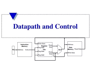
Next Address Logic Single-Cycle: Instruction Fetch Datapath • Instruction fetch • Inst. In instr. memory • program counter pointsto current instruction • adder increments PCto point to next inst. • For branch inst., the nextinst. address may not bevalid Read address Instruction Inst memory
31 26 21 16 11 6 0 op rs rt rd shamt funct 6 bits 5 bits 5 bits 5 bits 5 bits 6 bits R-typeDatapath • R[rd] <- R[rs] op R[rt] Example: add rd, rs, rt • Ra, Rb, and Rw come from instruction’s rs, rt, and rd fields • ALUctr and RegWr: control logic after decoding the instruction Rd Rs Rt ALU control Write 5 5 5 Read data 1 Rw R1 R2 Write data 32 32 32-bit Registers Result ALU 32 32 Read data 2 Clk 32
Next Address Logic Complete R-type Datapath ALU control Read register1 read data 1 zero Read register2 Read address result register file Instruction read data 2 Write register write data Inst memory Write
Timing: One complete cycle Clk Clk-to-Q Old Value New Value PC Instruction Memory Access Time Rs, Rt, Rd, Op, Func Old Value New Value Delay through Control Logic ALUctr Old Value New Value RegWr Old Value New Value Register File Access Time Read data 1& 2 Old Value New Value Reg setup ALU Delay Write data Old Value New Value Rd Rs Rt ALUctr Register Write Occurs Here RegWr 5 5 5 Read data 1 Rw Ra Rb Write data 32 Result 32 32-bit Registers ALU 32 32 Read data 2 Clk 32
Load/Store Datapathfetch same as R • lw $1, offset-value($2) ; sw $1, offset-value($2) • register file (get base reg.) • ALU to calculate memory address • data memory: read OR write • sign extension (offset ext.) data memory Read data1 rg 1 read data2 rg2 Write reg write data address write data read data Register file sign ext. 32 16
Branch Inst. Datapath Branch target • beq $1, $2, offset • if ($1=$2) goto PC+offset*4 • ALU for branch condition • Adder for computing branchtarget address • Shift left 2: increasesthe range of offset by 4 • Zero: control logic todecide if branch. Add shift left 2 Registers zero Read Reg 1 Data1 ALU Inst. To branch control logic Read Reg 2 Data2 32 ALU control sign ext. 16
M A d d u x A L U 4 A d d r e s u l t S h i f t t 2 l e f R e g i s t e r s R e a d R e a d r e g i s t e r 1 P C R e a d a d d r e s s R e a d d a t a 1 Z e r o r e g i s t e r 2 A L U I n s t r u c t i o n A L U R e a d A d d r e s s W r i t e R e a d r e s u l t M d a t a r e g i s t e r M d a t a 2 u I n s t r u c t i o n u x W r i t e D a t a x m e m o r y d a t a m e m o r y W r i t e d a t a 3 2 1 6 S i g n e x t e n d Complete Datapath for : R, LD/ST, BEQ Executes basic instructions in single clock cycle Any resource can only be once during a single cycle
Datapath controlled by control unit Identify your controls Identify your controls
Single-Cycle: Control Signals • Control: • input: 6-bit opcode • output: 9 control lines • ALU control: • input: ALUop + 6-bit (function field) • output: 3 lines • I, J type, ALU control depends on only ALUop Main op func
ALU Control, Truth Table *ALUop: output of main control R-: ALUop=10, lw/sw: ALUop=00 *ALU Control: combinational logic 8 inputs, 3 output.
Datapath timings in psec 30 100 100 400 200 120 350 30 30 50 Regfile Setup time Rformat timing= 400 +200+30 +120 +30 + 50 (IF WB) OR = 400 + 100 (IF – cntl – Pcmux)
Control Unit -- Control Signal Definitions PCsrc = branch AND zero
Example 1: Execution flow for add $1, $1, $3 (4 steps + bypass) 1. IF 1. IF 3. EX, ALU func. 2.D 4.Bypass 1. IF 5 5. WB write back result
Example 2: LW S0, OFF(S1)Memory address = OFF + S1 1. IF 3. EX, calc address 2.D 4.Mem rd OFF 5. WB write back result
Example 3: BEQ S1, S0, cs330target address = PC + offset x 4 Update PC with target addr. If successful 1. IF 3. EX, compare s1:s0 2.D
Single-Cycle: J-type • So far, datapath can handle R-type, lw/sw, beq • How about J-type? • J-type j L1 P.372jal L1 Exercise 5.6address=current PC =Actual address L1 =
What’s wrong with Single cycle CPI=1 processor? Arithmetic & Logical Inst Memory Reg File ALU RegW Load Inst Memory Reg File ALU Data Mem RegW Critical Path Store Inst Memory Reg File ALU Data Mem Branch Inst Memory Reg File cmp • Long Cycle Time • All instructions take as much time as the slowest • Real memory is slow
Single Cycle Timing Diagram Cycle 1 Cycle 2 Clk Single Cycle Implementation: Load Store Waste
CPU VS Microcontroller Microcontroller = CPU + Flash(ROM) + RAM + popular I/O peripherals. 8051 Microcontroller Block Diagram: Used in Lab project Used to implement low cost applications & Embedded Systems Eg automotive, appliances, elevators