The Processor: Datapath and Control
The Processor: Datapath and Control. Outline. Goals in processor implementation Brief review of sequential logic design Pieces of the processor implementation puzzle A simple implementation of a MIPS integer instruction subset Datapath Control logic design

The Processor: Datapath and Control
E N D
Presentation Transcript
The Processor: Datapath and Control
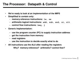
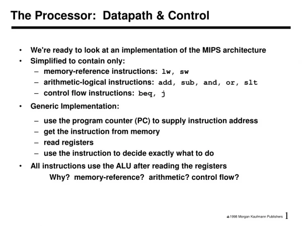
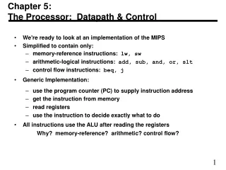
Outline • Goals in processor implementation • Brief review of sequential logic design • Pieces of the processor implementation puzzle • A simple implementation of a MIPS integer instruction subset • Datapath • Control logic design • A multi-cycle MIPS implementation • Datapath • Control logic design • Microcoded control • Exceptions • Some real microprocessor datapath and control
Goals in processor implementation • Balance the rate of supply of instructions and data and the rate at which the execution core can consume them and can update memory instruction supply execution core data supply
Goals in processor implementation • Recall from Chapter 2 • CPU Time = INST x CPI x CT • INST largely a function of the ISA and compiler • Objective: minimize CPI x CT within design constraints (cost, power, etc.) • Trading off CPI and CT is tricky multiplier multiplier multiplier logic logic logic
Brief review of sequential logic design • State elements are clocked devices • Flip flops, etc • Combinatorial elements hold no state • ALU, caches, multiplier, multiplexers, etc. • In edge triggered clocking, state elements are only updated on the (rising) edge of the clock pulse
Brief review of sequential logic design • The same state element can be read at the beginning of a clock cycle and updated at the end • Example: incrementing the PC clock 12 8 Add input 8 PC Add output 12 Add 4 PC register 8 12 clock
Our processor design progression • (1) Instruction fetch, execute, and operand reads from data memory all take place in a single clock cycle • (2) Instruction fetch, execute, and operand reads from data memory take place in successive clock cycles • (3) A pipelined design
Pieces of the processor puzzle • Instruction fetch • Execution • Data memory instruction supply execution core data supply
Instruction fetch datapath • Memory to hold instructions • Register to hold the instruction memory address • Logic to generate the next instruction address PC +4
Execution datapath • Focus on only a subset of all MIPS instructions • add, sub, and, or • lw, sw • slt • beq, j • For all instructions except j, we • Read operands from the register file • Perform an ALU operation • For all instructions except sw, beq, and j, we write a result into the register file
Execution datapath • Register file block diagram • Read register 1,2: source operand register numbers • Read data 1,2: source operands (32 bits each) • Write register: destination operand register number • Write data: data written into register file • RegWrite: when asserted, enables the writing of Write Data
Execution datapath • Datapath for R-type (add, sub, and, or, slt) • R-type instruction format: 31 26 25 21 20 16 15 11 10 6 5 0 op rs rt rd shamt funct
Execution datapath • Datapath for beq instruction • I-type instruction format: • Zero ALU output indicates if rs=rt (branch is taken/not taken) • Branch target address is the sign extended immediate left shifted two positions, and added to PC+4 31 26 25 21 20 16 15 0 op rs rt immediate
Data memory • Used for lw, sw (I-type format) • Block diagram • Address: memory location to be read or written • Read data: data out of the memory on a load • Write data: data into the memory on a store • MemRead: indicates a read operation is to be performed • MemWrite: indicates a write operation is to be performed
Execution datapath + data memory • Datapath for lw, sw • Address is the sign-extended immediate added to the source operand read out of the register file • sw: data written to memory from specified register • lw: data written to register file from specified memory address
Putting the pieces together • Single clock cycle for fetch, execute, and operand read from data memory • 3 MUXes • Register file operand or sign extended immediate to ALU • ALU or data memory output written to register file • PC+4 or branch target address written to PC register
Datapath for R-type instructions Example: add $4, $18, $30
Datapath for I-type ALU instructions Example: slti $7, $4, 100
Datapath for not taken beq instruction Example: beq $28, $13, EXIT
Datapath for taken beq instruction Example: beq $28, $13, EXIT
Datapath for load instruction Example: lw $8, 112($2)
Datapath for store instruction Example: sw $10, 0($3)
ALU operation control • ALU control input codes from Chapter 4 • Two steps to generate the ALU control input • Use the opcode to distinguish R-type, lw and sw, and beq • If R-type, use funct field to determine the ALU control input
ALU operation control • Opcode used to generate a 2-bit signal called ALUOp with the following encodings • 00: lw or sw, perform an ALU add • 01: beq, perform an ALU subtract • 10: R-type, ALU operation is determined by the funct field
Comparing instruction fields • Opcode, source registers, function code, and immediate fields always in same place • Destination register is • bits 15-11 (rd) for R-type • bits 20-16 (rt) for lw • MUX to select the right one 31 26 25 21 20 16 15 11 10 6 5 0 0 rs rt rd shamt funct R-type 31 26 25 21 20 16 15 0 beq 4 rs rt immediate (offset) 31 26 25 21 20 16 15 0 lw (sw) 35 (43) rs rt immediate (offset)
(0) (34) (43) (4) Main control unit design • Truth table
Adding support for jump instructions • J-type format • Next PC formed by shifting left the 26-bit target two bits and combining it with the 4 high-order bits of PC+4 • Now the next PC will be one of • PC+4 • beq target address • j target address • We need another MUX and control bit 31 26 25 0 2 target
Evaluation of the simple implementation • All instructions take one clock cycle (CPI = 1) • Assume the following worst case delays • Instruction memory: 4 time units • Data memory: 4 time units (read), 2 time units (write) • ALU: 4 time units • Adders: 3 time units • Register file: 2 time units (read), 1 time unit (write) • MUXes, sign extension, gates, and shifters: 1 time unit • Large disparity in worst case delays among instruction types • R-type: 4+2+1+4+1+1 = 13 time units • beq: 4+2+1+4+1+1+1 = 14 time units • j: 4+1+1 = 6 time units • store: 4+2+4+2 = 12 time units • load: 4+2+4+4+1+1 = 16 time units
Evaluation of the simple implementation • Disparity would be worse in a real machine • Even slower integer instructions (e.g., multiply/divide in MIPS) • Floating point instructions • Simple instructions take as long as complex ones
A multicycle implementation • Instruction fetch, register file access, etc occur in separate clock cycles • Different instruction types take different numbers of cycles to complete • Clock cycle time should be faster
High level view of datapath • New registers store results of each step • Not programmer visible! • Hardware can be shared • One ALU for PC+4, branch target calculation, EA calculation, and arithmetic operations • One memory for instructions and data
First two cycles for all instructions • Instruction fetch (1st cycle) • Load the instruction into the IR register • IR = Memory[PC] • Increment the PC • PC = PC+4 • Instruction decode and register fetch (2nd cycle) • Read register file locations rs and rt, results into the A and B registers • A=Reg[IR[25-21]] • B=Reg[IR[20-16]] • Calculate the branch target address and load into ALUOut • ALUOut = PC+(sign-extend (IR[15-0]) <<2)
Instruction fetch • IR=Mem[PC]
Instruction fetch • PC=PC+4
Instruction decode and register fetch • A=Reg[IR[25-21]], B=Reg[IR[20-16]]
Instruction decode and register fetch • ALUOut = PC+(sign-extend (IR[15-0]) <<2)
Additional cycles for R-type • Execution • ALUOut = A op B • Completion • Reg[IR[15-11]] = ALUOut
R-type execution cycle • ALUOut = A op B
R-type completion cycle • Reg[IR[15-11]] = ALUOut
Additional cycles for store • Address computation • ALUOut = A + sign-extend (IR[15-0]) • Memory access • Memory[ALUOut] = B
Store address computation cycle • ALUOut = A + sign-extend (IR[15-0])
Store memory access cycle • Memory[ALUOut] = B
Additional cycles for load • Address computation • ALUOut = A + sign-extend (IR[15-0]) • Memory access • MDR = Memory[ALUOut] • Read completion • Reg[IR[20-16]] = MDR
Load memory access cycle • MDR = Memory[ALUOut]