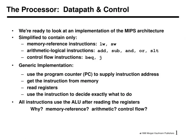
The Processor and its Datapath
The Processor and its Datapath. Define datapath Explain the function of various datapath elements Compare and contrast combinational elements with state elements. Define edge triggered clocking. Define the term program counter.

The Processor and its Datapath
E N D
Presentation Transcript
The Processor and its Datapath Define datapath Explain the function of various datapath elements Compare and contrast combinational elements with state elements. Define edge triggered clocking. Define the term program counter. Draw the datapath segment responsible for fetching instructions and incrementing the program counter. Define sign extend. Define branch target address
Datapath - A collection of datapath elements within a CPU that perform various data processing operations • Datapath Element • A functional unit used to operate on or hold datawithin a processor • Elements that operate on data are all combinational elements • Elements that hold data are state elements CS2710 Computer Organization
Combinational Elements • The output of a combinational element depends only on the current input(s) • No “memory” of past inputs • Given the same input, a combinational element always produces the same output • In MIPS, nearly all inputs and outputs are 32 bits wide X 32 X+Y 32 Y 32 CS2710 Computer Organization
State Elements • Output(s) depends on both input(s) and current state • Contain internal storage • Internal state may be lost on power loss • Internal state can be saved and restored 0x00400a0 0x3c011001(differs based on what is in instruction memory) CS2710 Computer Organization
A clocking methodology defines when signals (inputs and outputs) can be read and written • Edge Triggered Clocking • A clocking scheme in which all state changes occur on a clock edge • One of the clock edges (rising or falling) is chosen to be the active clock edge (by the designers) • States are stable at the active clock edge, and in transition between • The Clock cycle time is determined by the slowest datapath operation • Since every datapath element takes some finite amount of time to function Read Write Risingclock edge Clock cycle CS2710 Computer Organization Show rising and falling edges
Multiple clock cycles are needed for operations involving multiple state elements Read Read Write Write Clock cycle Clock cycle CS2710 Computer Organization Show rising and falling edges
More datapath elements • Program counter (PC) • A special-purpose register containing the address of the instruction in the program being executed • Sign extender • Increases the size of a data item (e.g. from 16 to 32 bits) by replicating the high order sign bit of the original data item to the high order bits of the larger destination data item 0x00400a0 0x00400a0 Write Read 0xf3a0 0xfffff3a0 Write Read 0x74b2 0x000074b2 CS2710 Computer Organization
ALU: Arithmetic/Logic Unit • Arithmetic • Logical comparison • Load from memory to register • Store from register to memory • Branching CS2710 Computer Organization
First step in executing an instruction: Instruction Fetch Determines the next instruction to execute; takes 1 cycle 0x004000a4 (next instruction address) Note: The signal going back to thePC is greatly simplified here. The actual signal is more complex. Start of clock cycle End of clock cycle 0x004000a0 0x3c011001 0xc421002c(next instruction Code) CS2710 Computer Organization
0 17 18 8 0 32 6 bits 5 bits 5 bits 5 bits 5 bits 6 bits Step 2: Instruction Decode and Register Fetch • Consider add $t1, $s1, $s2whose instruction code is 0x2824820 • Extract register numbers (17,18,8) • Extract part of op and funct (0, 32) and recombine as 4-bit ALU Opcode • Present to ALU (not shown) • Takes 1 cycle ALU Opcode for add 17 18 Value in $17 8 32-bit result to be placed in $8 will arrive here in 2 morecycles Value in $18
Step 3: Execute • Perform operation (in this example, add $t1, $s1, $s2) • The ALU adds the values in $17 and $18 presented to it from the Instruction Decode/Register Fetch of Step 2 • Takes 1 cycle ALU Opcode for add 17 18 Value in $17 8 32-bit result to be placed in $8 in asubsequent cycle 32-bit result to be placed in $8 will arrive here in asubsequent cycle Value in $18
Step 4: Memory access • In add $t1, $s1, $s2, memory is not accessed. • Instead: consider sw$t1, ($s1), where the data at the memory address contained in $s1 needs to be stored (or fetched, as in the case of lw) • The ALU sends the data in $t1 to the address stored in $s1, which takes 1 cycle • For lw, the ALU fetches the data from memory into a cache • Although add does not access memory, 1 cycle is still consumed (idle) • ALL instructions consume 1 cycle for step 4, whether they access memory or not! • This is done uniformly for all instructions for uniformity so that every instruction takes 5 steps ALU Opcode for sw 17 Address in $17 8 Addr in $17 Not used Value in $8
Step 5: Register writeback • Back toadd $t1, $s1, $s2 • The result from the add is written back to $8 ($t1) in step 5 • For an sw instruction, nothing happens in this cycle • For an lwinstrcution, the value is transferred from the cache to $8 • Consumes 1 cycle in all cases ALU Opcode 17 18 Value in $17 8 32-bit result of add Value in $18
A complete instruction in MIPS requires 5 steps/cycles. This is true for all instructions, whether the instruction needs to do something in each step or not! CS2710 Computer Organization
Example times for various datapath element functions (step times) • If executed sequentially, requires a total time of 800ps • …and, the step times are non-uniform! CS2710 Computer Organization