Building Processor Datapath and Control System
Learn about processor datapath and control, ALU operations, memory access, instruction format, control signals, opcode control, and execution phases.

Building Processor Datapath and Control System
E N D
Presentation Transcript
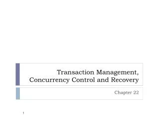
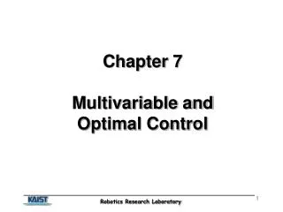
P C S r c M A d d u x A L U A d d 4 r e s u l t S h i f t l e f t 2 R e g i s t e r s A L U o p e r a t i o n 3 R e a d M e m W r i t e A L U S r c R e a d r e g i s t e r 1 P C R e a d a d d r e s s R e a d M e m t o R e g d a t a 1 Z e r o r e g i s t e r 2 I n s t r u c t i o n A L U A L U R e a d W r i t e R e a d A d d r e s s r e s u l t M d a t a r e g i s t e r d a t a 2 M u I n s t r u c t i o n u x W r i t e m e m o r y D a t a x d a t a m e m o r y W r i t e R e g W r i t e d a t a 3 2 1 6 S i g n M e m R e a d e x t e n d Building the Datapath • Use multiplexors to stitch them together
Control • Selecting the operations to perform (ALU, read/write, etc.) • Controlling the flow of data (multiplexor inputs) • Information comes from the 32 bits of the instruction • Example: add $8, $17, $18 Instruction Format: 000000 10001 10010 01000 00000 100000 op rs rt rd shamt funct • ALU's operation based on instruction type and function code
Control • e.g., what should the ALU do with this instruction • Example: lw $1, 100($2) 35 2 1 100 op rs rt 16 bit offset • ALU control input000 AND 001 OR 010 add 110 subtract 111 set-on-less-than • Why is the code for subtract 110 and not 011?
ALU Operation • For load and store instruction, use ALU add to compute memory address. • For R-type instruction, the operation of ALU will be determined by the funct filed, or the lower 6 bits of the 32-bit instruction. • For branch instructions, use ALU subtraction.
ALUOp computed from instruction type Control • Must describe hardware to compute 3-bit ALU control input • given instruction type 00 = lw, sw 01 = beq, 10 = arithmetic • function code for arithmetic • An example of multiple level decoding methodology.
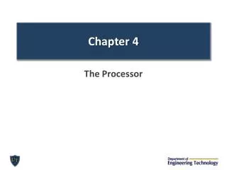
0 M u x A L U A d d 1 r e s u l t A d d R e g D s t 4 B r a n c h M e m R e a d M e m t o R e g I n s t r u c t i o n [ 3 1 2 6 ] C o n t r o l A L U O p M e m W r i t e A L U S r c R e g W r i t e I n s t r u c t i o n [ 2 5 2 1 ] R e a d R e a d r e g i s t e r 1 P C R e a d a d d r e s s d a t a 1 I n s t r u c t i o n [ 2 0 1 6 ] R e a d I n s t r u c t i o n 0 R e g i s t e r s R e a d [ 3 1 0 ] 0 W r i t e M d a t a 2 I n s t r u c t i o n r e g i s t e r u m e m o r y x W r i t e 1 d a t a 0 1 6 3 2 I n s t r u c t i o n [ 1 5 0 ] I n s t r u c t i o n [ 5 0 ] Control S h i f t l e f t 2 Z e r o r e g i s t e r 2 A L U A L U R e a d A d d r e s s r e s u l t 1 d a t a M M u u I n s t r u c t i o n [ 1 5 1 1 ] x D a t a x 1 m e m o r y W r i t e d a t a S i g n e x t e n d A L U c o n t r o l
Control and Opcode • Will use 6 bit opcodes to set the nine control signals • Figure 5.27 shows the relationship.
Control • Simple combinational logic (truth tables)
0 M u x A L U A d d 1 r e s u l t A d d R e g D s t 4 B r a n c h M e m R e a d M e m t o R e g I n s t r u c t i o n [ 3 1 2 6 ] C o n t r o l A L U O p M e m W r i t e A L U S r c R e g W r i t e I n s t r u c t i o n [ 2 5 2 1 ] R e a d R e a d r e g i s t e r 1 P C R e a d a d d r e s s d a t a 1 I n s t r u c t i o n [ 2 0 1 6 ] R e a d I n s t r u c t i o n 0 R e g i s t e r s R e a d [ 3 1 0 ] 0 W r i t e M d a t a 2 I n s t r u c t i o n r e g i s t e r u m e m o r y x W r i t e 1 d a t a 0 1 6 3 2 I n s t r u c t i o n [ 1 5 0 ] I n s t r u c t i o n [ 5 0 ] R-type Instruction Execution Phases • Fetch instruction from memory, increase PC S h i f t l e f t 2 Z e r o r e g i s t e r 2 A L U A L U R e a d A d d r e s s r e s u l t 1 d a t a M M u u I n s t r u c t i o n [ 1 5 1 1 ] x D a t a x 1 m e m o r y W r i t e d a t a S i g n e x t e n d A L U c o n t r o l
0 M u x A L U A d d 1 r e s u l t A d d R e g D s t 4 B r a n c h M e m R e a d M e m t o R e g I n s t r u c t i o n [ 3 1 2 6 ] C o n t r o l A L U O p M e m W r i t e A L U S r c R e g W r i t e I n s t r u c t i o n [ 2 5 2 1 ] R e a d R e a d r e g i s t e r 1 P C R e a d a d d r e s s d a t a 1 I n s t r u c t i o n [ 2 0 1 6 ] R e a I n s t r u c t i o n 0 R e g i s t e r s R e a d [ 3 1 0 ] 0 W r i t e M d a t a 2 I n s t r u c t i o n r e g i s t e r u m e m o r y x W r i t e 1 d a t a 0 1 6 3 2 I n s t r u c t i o n [ 1 5 0 ] I n s t r u c t i o n [ 5 0 ] Phase 2 • Read from two registers S h i f t l e f t 2 d Z e r o r e g i s t e r 2 A L U A L U R e a d A d d r e s s r e s u l t 1 d a t a M M u u I n s t r u c t i o n [ 1 5 1 1 ] x D a t a x 1 m e m o r y W r i t e d a t a S i g n e x t e n d A L U c o n t r o l
0 M u x A L U A d d 1 r e s u l t A d d R e g D s t 4 B r a n c h M e m R e a d M e m t o R e g I n s t r u c t i o n [ 3 1 2 6 ] C o n t r o l A L U O p M e m W r i t e A L U S r c R e g W r i t e I n s t r u c t i o n [ 2 5 2 1 ] R e a d P C R e a d a d d r e s s d a t a 1 I n s t r u c t i o n [ 2 0 1 6 ] I n s t r u c t i o n 0 R e g i s t e r s R e a d [ 3 1 0 ] 0 W r i t e M d a t a 2 I n s t r u c t i o n r e g i s t e r u m e m o r y x W r i t e 1 d a t a 0 1 6 3 2 I n s t r u c t i o n [ 1 5 0 ] A L U c o n t r o l I n s t r u c t i o n [ 5 0 ] Phase 3 • ALU operation S h i f t l e f t 2 R e a d r e g i s t e r 1 R e a d Z e r o r e g i s t e r 2 A L U A L U R e a d A d d r e s s r e s u l t 1 d a t a M M u u I n s t r u c t i o n [ 1 5 1 1 ] x D a t a x 1 m e m o r y W r i t e d a t a S i g n e x t e n d
0 M u x A L U A d d 1 r e s u l t A d d S h i f t l e f t 2 R e g D s t 4 B r a n c h M e m R e a d M e m t o R e g I n s t r u c t i o n [ 3 1 2 6 ] C o n t r o l A L U O p M e m W r i t e A L U S r c R e g W r i t e I n s t r u c t i o n [ 2 5 2 1 ] R e a d P C R e a d a d d r e s s d a t I n s t r u c t i o n [ 2 0 1 6 ] I n s t r u c t i o n 0 R e g i s t e r s [ 3 1 0 ] 0 W r i t e M I n s t r u c t i o n r e g i s t e r u m e m o r y x W r i t e 1 d a t a 0 1 6 3 2 I n s t r u c t i o n [ 1 5 0 ] A L U c o n t r o l I n s t r u c t i o n [ 5 0 ] Phase 4 • Write result to register. R e a d r e g i s t e r 1 a 1 R e a d Z e r o r e g i s t e r 2 A L U R e a d A L U R e a d d a t a 2 A d d r e s s r e s u l t 1 d a t a M M u u I n s t r u c t i o n [ 1 5 1 1 ] x D a t a x 1 m e m o r y W r i t e d a t a S i g n e x t e n d
Our Simple Control Structure • All of the logic is combinational • We wait for everything to settle down, and the right thing to be done • ALU might not produce right answer right away • we use write signals along with clock to determine when to write • Cycle time determined by length of the longest path
M A d d u x 0 4 R e g W r i t e I n s t r u c t i o n [ 2 5 2 1 ] R e a d r e g i s t e r 1 R e a d M e m W r i t e R e a d P C d a t a 1 I n s t r u c t i o n [ 2 0 1 6 ] a d d r e s s R e a d M e m t o R e g A L U S r c r e g i s t e r 2 Z e r o I n s t r u c t i o n R e a d A L U [ 3 1 0 ] R e a d W r i t e d a t a 2 1 A d d r e s s r e s u l t r e g i s t e r d a t a M I n s t r u c t i o n W r i t e u m e m o r y R e g i s t e r s x d a t a D a t a 0 W r i t e m e m o r y R e g D s t d a t a 1 6 3 2 S i g n I n s t r u c t i o n [ 1 5 0 ] e x t e n d M e m R e a d I n s t r u c t i o n [ 5 0 ] A L U O p Single Cycle Implementation • Calculate cycle time assuming negligible delays except: • memory (2ns), ALU and adders (2ns), register file access (1ns) • look at the example in the last part of Sec 5.3 P C S r c 1 A L U A d d r e s u l t S h i f t l e f t 2 1 A L U 1 M M u u I n s t r u c t i o n [ 1 5 1 1 ] x x 0 0 A L U c o n t r o l
Where we are headed • Single Cycle Problems: • what if we had a more complicated instruction like floating point? • wasteful of area • One Solution: • use a smaller cycle time • have different instructions take different numbers of cycles • a multicycle datapath
Multicycle Approach • We will be reusing functional units • ALU used to compute address and to increment PC • Memory used for instruction and data • Introduce new registers in main functional units • IR for storing instruction, MDR for storing data read from memory • A, B registers for storing data read from registers • ALUOut register for storing ALU results • Our control signals will not be determined solely by instruction • We will use a finite state machine for control.
Review: finite state machines • Finite state machines: • a set of states and • next state function (determined by current state and the input) • output function (determined by current state and possibly input) • We’ll use a Moore machine (output based only on current state) N e x t s t a t e N e x t - s t a t e C u r r e n t s t a t e f u n c t i o n C l o c k I n p u t s O u t p u t O u t p u t s f u n c t i o n
Review: finite state machines • Example: • Output: NSLite, EWLite • State: NSGreen, EWGreen • Input: NSCar, EWCar B. 28: State Diagram
Multicycle Approach • Break up the instructions into steps, each step takes a cycle • balance the amount of work to be done • restrict each cycle to use only one major functional unit • At the end of a cycle • store values for use in later cycles (easiest thing to do) • introduce additional internal registers • Need more multiplexors since we are sharing functional units (ALU, memory). • Justified since cost of registers and multiplexor is much less than ALU or memory.
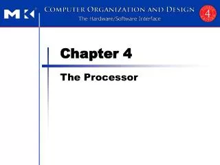
P C 0 0 I n s t r u c t i o n R e a d M M A [ 2 5 2 1 ] r e g i s t e r 1 u u x x R e a d A I n s t r u c t i o n R e a d Z e r o M e m o r y 1 d a t a 1 1 [ 2 0 1 6 ] r e g i s t e r 2 A L U A L U A L U O u t 0 M e m D a t a R e g i s t e r s r e s u l t I n s t r u c t i o n W r i t e M R e a d [ 1 5 0 ] r e g i s t e r B u 0 d a t a 2 I n s t r u c t i o n W r i t e x [ 1 5 1 1 ] M I n s t r u c t i o n 4 1 W r i t e d a t a 1 u r e g i s t e r d a t a 2 x 0 I n s t r u c t i o n 3 [ 1 5 0 ] M u x M e m o r y 1 1 6 3 2 d a t a S h i f t S i g n r e g i s t e r l e f t 2 e x t e n d MIPS Multicycle Datapath • handling basic instructions d d r e s s
I o r D M e m R e a d M e m W r i t e R e g D s t R e g W r i t e P C 0 I n s t r u c t i o n R e a d M [ 2 5 2 1 ] r e g i s t e r 1 u x R e a d I n s t r u c t i o n R e a d d a t a 1 M e m o r y 1 [ 2 0 1 6 ] r e g i s t e r 2 0 M e m D a t a R e g i s t e r s I n s t r u c t i o n W r i t e R e a d M [ 1 5 0 ] r e g i s t e r d a t a 2 u I n s t r u c t i o n W r i t e x M [ 1 5 1 1 ] I n s t r u c t i o n 4 1 W r i t e d a t a 1 u r e g i s t e r d a t a 0 I n s t r u c t i o n [ 1 5 0 ] M u x 1 1 6 3 2 S h i f t S i g n l e f t 2 e x t e n d I n s t r u c t i o n [ 5 0 ] M e m t o R e g A L U S r c B A L U O p Multicycle Datapath (with control signals) I R W r i t e A L U S r c A 0 M A d d r e s s u x A Z e r o 1 A L U A L U A L U O u t r e s u l t B 0 2 x 3 M e m o r y d a t a A L U r e g i s t e r c o n t r o l
P C W r i t e C o n d P C S o u r c e P C W r i t e A L U O p O u t p u t s I o r D A L U S r c B M e m R e a d A L U S r c A C o n t r o l M e m W r i t e R e g W r i t e M e m t o R e g O p R e g D s t I R W r i t e [ 5 0 ] 0 M u J u m p x I n s t r u c t i a d d r e s s [ 3 1 - 0 ] 2 I n s t r u c t i o n [ 3 1 - 2 6 ] P C 0 I n s t r u c t i o n R e a d M [ 2 5 2 1 ] r e g i s t e r 1 u x R e a d A I n s t r u c t i o n R e a d Z e r o 1 d a t a 1 [ 2 0 1 6 ] r e g i s t e r 2 A L U A L U 0 R e g i s t e r s r e s u l t I n s t r u c t i o n W r i t e M R e a d B [ 1 5 0 ] r e g i s t e r u I n s t r u c t i o n d a t a 2 x [ 1 5 1 1 ] I n s t r u c t i o n 4 W r i t e 1 r e g i s t e r d a t a 0 I n s t r u c t i o n [ 1 5 0 ] M u x M e m o r y 1 1 6 3 2 d a t a A L U S h i f t S i g n r e g i s t e r c o n t r o l l e f t 2 e x t e n d I n s t r u c t i o n [ 5 0 ] Multicycle Datapath (complete) 1 2 6 2 8 o n [ 2 5 0 ] S h i f t l e f t 2 P C [ 3 1 - 2 8 ] 0 M A d d r e s s u x M e m o r y 1 A L U O u t M e m D a t a 0 W r i t e M 1 d a t a u 2 x 3
Five Execution Steps • Instruction Fetch • Instruction Decode and Register Fetch • Execution, Memory Address Computation, or Branch Completion • Memory Access or R-type instruction completion • Write-back step INSTRUCTIONS TAKE FROM 3 - 5 CYCLES!
Step 1: Instruction Fetch • Use PC to get instruction and put it in the Instruction Register. • Increment the PC by 4 and put the result back in the PC. • Can be described succinctly using RTL "Register-Transfer Language" IR = Memory[PC]; PC = PC + 4;Can we figure out the values of the control signals?What is the advantage of updating the PC now?
Step 2: Instruction Decode and Register Fetch • Read registers rs and rt in case we need them • Compute the branch address in case the instruction is a branch • RTL: A = Reg[IR[25-21]]; B = Reg[IR[20-16]]; ALUOut = PC + (sign-extend(IR[15-0]) << 2); • We aren't setting any control lines based on the instruction type (we are busy "decoding" it in our control logic)
Step 3 (instruction dependent) • ALU is performing one of three functions, based on instruction type • Memory Reference: ALUOut = A + sign-extend(IR[15-0]); • R-type: ALUOut = A op B; • Branch: if (A==B) PC = ALUOut;
Step 4 (R-type or memory-access) • Loads and stores access memory MDR = Memory[ALUOut]; or Memory[ALUOut] = B; • R-type instructions finish Reg[IR[15-11]] = ALUOut;The write actually takes place at the end of the cycle on the edge
Write-back step • Reg[IR[20-16]]= MDR;
Simple Questions • How many cycles will it take to execute this code? lw $t2, 0($t3) lw $t3, 4($t3) beq $t2, $t3, Label #assume not add $t5, $t2, $t3 sw $t5, 8($t3)Label: ... • What is going on during the 8th cycle of execution? • In what cycle does the actual addition of $t2 and $t3 takes place?
Implementing the Control • Value of control signals is dependent upon: • what instruction is being executed • which step is being performed • Use the information we accumulated to specify a finite state machine • specify the finite state machine graphically, or • use microprogramming • Implementation can be derived from specification
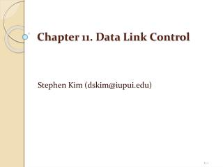
I n s t r u c t i o n d e c o d e / I n s t r u c t i o n f e t c h r e g i s t e r f e t c h M e m R e a d A L U S r c A = 0 I o r D = 0 A L U S r c A = 0 I R W r i t e A L U S r c B = 1 1 A L U S r c B = 0 1 A L U O p = 0 0 A L U O p = 0 0 P C W r i t e P C S o u r c e = 0 0 R = p O ( ) ' W M e m o r y a d d r e s s S ' B r a n c h = J u m p p O c o m p u t a t i o n ( r o E x e c u t i o n c o m p l e t i o n ) c o m p l e t i o n ' W L ' = p O ( A L U S r c A = 1 A L U S r c A = 1 A L U S r c B = 0 0 A L U S r c A = 1 P C W r i t e A L U S r c B = 1 0 A L U O p = 0 1 A L U S r c B = 0 0 P C S o u r c e = 1 0 A L U O p = 0 0 P C W r i t e C o n d A L U O p = 1 0 P C S o u r c e = 0 1 M e m o r y M e m o r y a c c e s s a c c e s s R - t y p e c o m p l e t i o n R e g D s t = 1 M e m R e a d M e m W r i t e R e g W r i t e I o r D = 1 I o r D = 1 M e m t o R e g = 0 W r i t e - b a c k s t e p R e g D s t = 0 R e g W r i t e M e m t o R e g = 1 Graphical Specification of FSM 0 1 • How many state bits will we need? S t a r t ) ' ) e Q ) p ' y t E J - ' B ' = = p p O O ( ( 2 6 8 9 ( ) O ' p W = L ' ' S = W ' ) p O ( 3 5 7 4
Finite State Machine for Control • Implementation:
PLA Implementation • If I picked a horizontal or vertical line could you explain it?
m n ROM Implementation • ROM = "Read Only Memory" • values of memory locations are fixed ahead of time • A ROM can be used to implement a truth table • if the address is m-bits, we can address 2m entries in the ROM. • our outputs are the bits of data that the address points to.m is the "height", and n is the "width" 0 0 0 0 0 1 1 0 0 1 1 1 0 0 0 1 0 1 1 0 0 0 1 1 1 0 0 0 1 0 0 0 0 0 0 1 0 1 0 0 0 1 1 1 0 0 1 1 0 1 1 1 0 1 1 1
ROM Implementation • How many inputs are there? 6 bits for opcode, 4 bits for state = 10 address lines (i.e., 210 = 1024 different addresses) • How many outputs are there? 16 datapath-control outputs, 4 state bits = 20 outputs • ROM is 210 x 20 = 20K bits (and a rather unusual size) • Rather wasteful, since for lots of the entries, the outputs are the same ?i.e., opcode is often ignored
ROM vs PLA • Break up the table into two parts ?4 state bits tell you the 16 outputs, 24 x 16 bits of ROM ?10 bits tell you the 4 next state bits, 210 x 4 bits of ROM ?Total: 4.3K bits of ROM • PLA is much smaller ?can share product terms ?only need entries that produce an active output ?can take into account don't cares • Size is (#inputs #product-terms) + (#outputs #product-terms) For this example = (10x17)+(20x17) = 460 PLA cells • PLA cells usually about the size of a ROM cell (slightly bigger)
Another Implementation Style • Complex instructions: the "next state" is often current state + 1
Microprogramming • What are the microinstructions?
Microprogramming • A specification methodology • appropriate if hundreds of opcodes, modes, cycles, etc. • signals specified symbolically using microinstructions • What would a microassembler do?
Maximally vs. Minimally Encoded • No encoding: • 1 bit for each datapath operation • faster, requires more memory (logic) • used for VAX 780 an astonishing 400K of memory! • Lots of encoding: • send the microinstructions through logic to get control signals • uses less memory, slower • Historical context of CISC: • Too much logic to put on a single chip with everything else • Use a ROM (or even RAM) to hold the microcode • It’s easy to add new instructions
Microcode: Trade-offs • Distinction between specification and implementation is sometimes blurred • Specification Advantages: • Easy to design and write • Design architecture and microcode in parallel • Implementation (off-chip ROM) Advantages • Easy to change since values are in memory • Can emulate other architectures • Can make use of internal registers • Implementation Disadvantages, SLOWER now that: • Control is implemented on same chip as processor • ROM is no longer faster than RAM • No need to go back and make changes