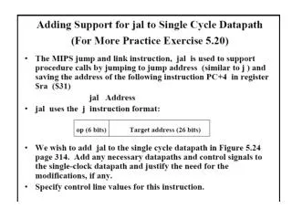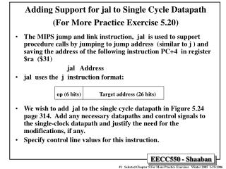
Adding Support for jal to Single Cycle Datapath (For More Practice Exercise 5.20)
270 likes | 2.7k Vues
op (6 bits) Target address (26 bits). Adding Support for jal to Single Cycle Datapath (For More Practice Exercise 5.20).

Adding Support for jal to Single Cycle Datapath (For More Practice Exercise 5.20)
E N D
Presentation Transcript
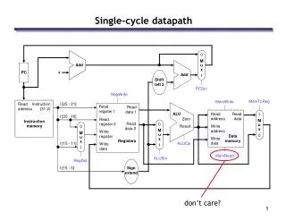
op (6 bits) Target address (26 bits) Adding Support for jal to Single Cycle Datapath(For More Practice Exercise 5.20) • The MIPS jump and link instruction, jal is used to support procedure calls by jumping to jump address (similar to j ) and saving the address of the following instruction PC+4 in register $ra ($31) jal Address • jal uses the j instruction format: • We wish to add jal to the single cycle datapath in Figure 5.24 page 314. Add any necessary datapaths and control signals to the single-clock datapath and justify the need for the modifications, if any. • Specify control line values for this instruction.
Exercise 5.20: jump and link, jal support to Single Cycle Datapath Instruction Word ¬ Mem[PC] R[31] ¬ PC + 4 PC ¬ Jump Address Jump Address PC + 4 PC + 4 Branch Target PC + 4 rs R[rs] rt R[rt] 31 2 2 rd imm16 (For More Practice Exercise 5.20)
Exercise 5.20: jump and link, jal support to Single Cycle Datapath Adding Control Lines Settings for jal(For Textbook Single Cycle Datapath including Jump) RegDst Is now 2 bits MemtoReg Is now 2 bits Memto- Reg Mem Mem RegDst ALUSrc Reg Write Read Write Branch ALUOp1 ALUOp0 Jump R-format 01 0 00 1 0 0 0 1 0 0 lw 00 1 01 1 1 0 0 0 0 0 sw xx 1 xx 0 0 1 0 0 0 0 beq xx 0 xx 0 0 0 1 0 1 0 J xx x xx 0 0 0 x x x 1 JAL 10 x 10 1 0 0 x x x 1 R[31] PC+ 4 PC ¬ Jump Address Instruction Word ¬ Mem[PC] R[31] ¬ PC + 4 PC ¬ Jump Address (For More Practice Exercise 5.20)
Adding Support for LWR to Single Cycle Datapath(For More Practice Exercise 5.22) • We wish to add a variant of lw (load word) let’s call it LWR to the single cycle datapath in Figure 5.24 page 314. LWR $rd, $rs, $rt • The LWR instruction is similar to lw but it sums two registers (specified by $rs, $rt) to obtain the effective load address and uses the R-Type format • Add any necessary datapaths and control signals to the single cycle datapath and justify the need for the modifications, if any. • Specify control line values for this instruction. (For More Practice Exercise 5.22)
Adding Control Lines Settings for LWR(For Textbook Single Cycle Datapath including Jump) Exercise 5.22: LWR (R-format LW) support to Single Cycle Datapath Instruction Word ¬ Mem[PC] PC ¬ PC + 4 R[rd] ¬ Mem[ R[rs] + R[rt] ] No new components or connections are needed for the datapath just the proper control line settings Memto- Reg Mem Mem RegDst ALUSrc Reg Write Read Write Branch ALUOp1 ALUOp0 Jump R-format 1 0 0 1 0 0 0 1 0 0 lw 0 1 1 1 1 0 0 0 0 0 sw x 1 x 0 0 1 0 0 0 0 beq x 0 x 0 0 0 1 0 1 0 J x x x 0 0 0 x x x 1 LWR 1 0 1 1 1 0 0 0 0 0 Add R[rt] rd (For More Practice Exercise 5.22)
6 bits 5 bits 5 bits 16 bits Not Used OP rs address rt Adding Support for jm to Single Cycle Datapath(Based on “For More Practice Exercise 5.44” but for single cycle) • We wish to add a new instruction jm (jump memory) to the single cycle datapath in Figure 5.24 page 314. jm offset($rs) • The jm instruction loads a word from effective address ($rs + offset), this is similar to lw except the loaded word is put in the PC instead of register $rt. • Jm used the I-format with field rt not used. • Add any necessary datapaths and control signals to the single cycle datapath and justify the need for the modifications, if any. • Specify control line values for this instruction.
Adding jump memory, jm support to Single Cycle Datapath Instruction Word ¬ Mem[PC] PC ¬ Mem[R[rs] + SignExt[imm16]] Jump 2 2 PC + 4 Jump 2 Branch Target rs R[rs] rt R[rt] rd imm16 (Based on “For More Practice Exercise 5.44” but for single cycle)
Adding jm support to Single Cycle Datapath Adding Control Lines Settings for jm(For Textbook Single Cycle Datapath including Jump) Jump is now 2 bits Memto- Reg Mem Mem RegDst ALUSrc Reg Write Read Write Branch ALUOp1 ALUOp0 Jump R-format 1 0 0 1 0 0 0 1 0 00 lw 0 1 1 1 1 0 0 0 0 00 sw x 1 x 0 0 1 0 0 0 00 beq x 0 x 0 0 0 1 0 1 00 J x x x 0 0 0 x x x 01 JAL x 1 x 0 1 0 x 0 0 10 add R[rs] PC ¬ Mem[R[rs] + SignExt[imm16]]
Adding Support for swap to Multi Cycle Datapath (For More Practice Exercise 5.42) • You are to add support for a new instruction, swap that exchanges the values of two registers to the MIPS multicycle datapath of Figure 5.28 on page 232 swap $rs, $rt • Swap used the R-Type format with: the value of field rs = the value of field rd • Add any necessary datapaths and control signals to the multicycle datapath. Find a solution that minimizes the number of clock cycles required for the new instruction without modifying the register file. Justify the need for the modifications, if any. • Show the necessary modifications to the multicycle control finite state machine of Figure 5.38 on page 339 when adding the swap instruction. For each new state added, provide the dependent RTN and active control signal values.
rs rt op rd [31-26] [25-21] [20-16] [10-6] 2 2 2 Adding swap Instruction Support to Multi Cycle Datapath We assume here rs = rd in instruction encoding Swap $rs, $rt R[rt] ¬ R[rs] R[rs] ¬ R[rt] PC+ 4 rs Branch Target R[rs] rt R[rt] rd imm16 The outputs of A and B should be connected to the multiplexor controlled by MemtoReg if one of the two fields (rs and rd) contains the name of one of the registers being swapped. The other register is specified by rt. The MemtoReg control signal becomes two bits. (For More Practice Exercise 5.42)
Adding swap Instruction Support to Multi Cycle Datapath IF A ¬ R[rs] B ¬ R[rt] ALUout ¬ PC + (SignExt(imm16) x4) ID IR ¬ Mem[PC] PC ¬ PC + 4 EX ALUout ¬ A + SignEx(Imm16) WB1 R[rd] ¬ B ALUout ¬ A func B WB2 Zero ¬ A -B Zero: PC ¬ ALUout R[rt] ¬ A R[rd] ¬ ALUout MEM WB Swap takes 4 cycles WB (For More Practice Exercise 5.42)
6 bits [31-26] 5 bits [25-21] 5 bits [20-16] 5 bits [15-11] 5 bits [4-0] 6 bits [10-5] add3 $s1 $s2 $s0 $s3 Not used OP rs rd rx rt Adding Support for add3 to Single Cycle Datapath(For More Practice Exercise 5.45) • You are to add support for a new instruction, add3, that adds the values of three registers, to the MIPS multicycle datapath of Figure 5.28 on page 232 For example: add3 $s0,$s1, $s2, $s3 Register $s0 gets the sum of $s1, $s2 and $s3. The instruction encoding uses a modified R-format, with an additional register specifier rx added replacing the five low bits of the “funct” field. • Add necessary datapath components, connections, and control signals to the multicycle datapath without modifying the register bank or adding additional ALUs. Find a solution that minimizes the number of clock cycles required for the new instruction. Justify the need for the modifications, if any. • Show the necessary modifications to the multicycle control finite state machine of Figure 5.38 on page 339 when adding the add3 instruction. For each new state added, provide the dependent RTN and active control signal values.
rs rt op rd [31-26] [25-21] [20-16] [10-6] [4-0] 2 2 rx Exercise 5.45: add3 instruction support to Multi Cycle Datapath Add3 $rd, $rs, $rt, $rx R[rd] ¬ R[rs] + R[rt] + R[rx] rx is a new register specifier in field [0-4] of the instruction No additional register read ports or ALUs allowed Modified R-Format WriteB 2 PC+ 4 rs Branch Target rt rx rd imm16 1. ALUout is added as an extra input to first ALU operand MUX to use the previous ALU result as an input for the second addition. 2. A multiplexor should be added to select between rt and the new field rx containing register number of the 3rd operand (bits 4-0 for the instruction) for input for Read Register 2. This multiplexor will be controlled by a new one bit control signal called ReadSrc. 3. WriteB control line added to enable writing R[rx] to B
Exercise 5.45: add3 instruction support to Multi Cycle Datapath IF A ¬ R[rs] B ¬ R[rt] ALUout ¬ PC + (SignExt(imm16) x4) ID IR ¬ Mem[PC] PC ¬ PC + 4 EX ALUout ¬ A + SignEx(Im16) WriteB EX1 ALUout ¬ A + B B ¬ R[rx] WriteB ALUout ¬ A func B EX2 Zero ¬ A -B Zero: PC ¬ ALUout ALUout ¬ ALUout + B R[rd] ¬ ALUout MEM WB Add3 takes 5 cycles WB (For More Practice Exercise 5.45)