Designing a Single Cycle Datapath for Computer Architecture Course
570 likes | 750 Vues
Learn how to design a single cycle processor, analyze MIPS instruction set, address modes, formats, and register transfer logic using RTL. Follow step-by-step process & understand performance metrics.

Designing a Single Cycle Datapath for Computer Architecture Course
E N D
Presentation Transcript
Designing a Single Cycle Datapath In this lecture, slides from lectures 3, 8 and 9 from the course Computer Architecture ECE 201 by Professor Mike Schulte are used with permission.
Processor Input Control Memory Datapath Output The Big Picture: Where are We Now? • The Five Classic Components of a Computer • Today’s Topic: Design a Single Cycle Processor
CPI Inst. Count Cycle Time The Big Picture: The Performance Perspective • Performance of a machine is determined by: • Instruction count • Clock cycle time • Clock cycles per instruction • Processor design (datapath and control) will determine: • Clock cycle time • Clock cycles per instruction • Single cycle processor - one clock cycle per instruction • Advantages: Simple design, low CPI • Disadvantages: Long cycle time, which is limited by the slowest instruction.
How to Design a Processor: step-by-step 1. Analyze instruction set => datapath requirements • the meaning of each instruction is given by register transfers R[rd] <– R[rs] + R[rt]; • datapath must include storage element for ISA registers • datapath must support each register transfer 2. Select set of datapath components and establish clocking methodology 3. Design datapath to meet the requirements 4. Analyze implementation of each instruction to determine setting of control points that effects the register transfer. 5. Design the control logic
31 26 21 16 11 6 0 op rs rt rd shamt funct 6 bits 5 bits 5 bits 5 bits 5 bits 6 bits 31 26 21 16 0 immediate op rs rt 6 bits 5 bits 5 bits 16 bits 31 26 0 op target address 6 bits 26 bits Review: The MIPS Instruction Formats • All MIPS instructions are 32 bits long. The three instruction formats are: • R-type • I-type • J-type • The different fields are: • op: operation of the instruction • rs, rt, rd: the source and destination register specifiers • shamt: shift amount • funct: selects the variant of the operation in the “op” field • address / immediate: address offset or immediate value • target address: target address of the jump instruction
Translating MIPS Assembly into Machine Language • Humans see instructions as words (assembly language), but the computer sees them as ones and zeros (machine language). • An assembler translates from assembly language to machine language. • For example, the MIPS instruction add $t0, $s1, $s2 is translated as follows (see back of book): Assembly Comment add op = 0, shamt = 0, funct = 32 $t0 rd = 8 $s1 rs = 17 $s2 rt = 18 000000 10001 10010 01000 00000 100000 op rs rt rd shamt funct
MIPS Addressing Modes • Addressing modes specify where the data used by an instruction is located. mode example action register direct add $s1, $s2, $s3 $s1 = $s2 + $s3 immediate addi $s1, $s2, 200 $s1 = $s2 + 200 base+index lw $s1, 200($s2) $s1 = mem[200 + $s2] PC-relative beq $s1, $s2, 200 if ($s1 == $s2) PC = PC+4+200*4 Pseudo-direct j 4000 PC = (PC[31:28], 4000*4) • Often, the type of addressing mode depends on the type of operation being performed (e.g., branches all use PC relative) • A summary of MIPS addressing modes is given on the back cover of the book.
MIPS Addressing Modes/Instruction Formats • All MIPS instructions are 32 bits wide - fixed length add $s1, $s2, $s3 Register (direct) op rs rt rd register Immediate addi $s1, $s2, 200 op rs rt immed Base+index op rs rt immed Memory register + lw $s1, 200($s2) PC-relative op rs rt immed Memory PC + beq $s1, $s2, 200
31 26 21 16 11 6 0 op rs rt rd shamt funct 6 bits 5 bits 5 bits 5 bits 5 bits 6 bits 31 26 21 16 0 op rs rt immediate 6 bits 5 bits 5 bits 16 bits 31 26 21 16 0 op rs rt immediate 6 bits 5 bits 5 bits 16 bits 31 26 21 16 0 op rs rt immediate 6 bits 5 bits 5 bits 16 bits Step 1a: The MIPS Subset for Today • ADD and SUB • addu rd, rs, rt • subu rd, rs, rt • OR Immediate: • ori rt, rs, imm16 • LOAD and STORE • lw rt, rs, imm16 • sw rt, rs, imm16 • BRANCH: • beq rs, rt, imm16
Register Transfer Logic (RTL) • RTL gives the meaning of the instructions • All instructions start by fetching the instruction op | rs | rt | rd | shamt | funct = MEM[ PC ] op | rs | rt | Imm16 = MEM[ PC ] inst Register Transfers addu R[rd] <– R[rs] + R[rt]; PC <– PC + 4 subu R[rd] <– R[rs] – R[rt]; PC <– PC + 4 ori R[rt] <– R[rs] + zero_ext(imm16); PC <– PC + 4 load R[rt] <– MEM[ R[rs] + sign_ext(imm16)]; PC <– PC + 4 store MEM[ R[rs] + sign_ext(imm16) ] <– R[rt]; PC <– PC + 4 beq if ( R[rs] == R[rt] ) then PC <– PC + 4 + sign_ext(imm16)] || 00 else PC <– PC + 4
Step 1: Requirements of the Instruction Set • Memory • instruction & data • Registers (32 x 32) • read rs • read rt • write rt or rd • PC • Extender (sign extend or zero extend) • Add and sub register or extended immediate • Add 4 or shifted extended immediate to PC
Step 2: Components of the Datapath CarryIn • Adder • MUX • ALU A 32 Sum Adder 32 B Carry 32 Select A 32 Combinational Logic:Does not use a clock Y MUX 32 B 32 OP 3 A 32 Result ALU 32 B 32
Storage Element: Register (Basic Building Blocks) • Register • Similar to the D Flip Flop except • N-bit input and output • Write enable input • Write Enable: • negated (0): Data Out will not change • asserted (1): Data Out will become Data In on the falling edge of the clock Write Enable Data In Data Out N N Clk
. . . . . . . . . . . . Clocking Methodology - Negative Edge Triggered Clk Setup Hold Setup Hold Don’t Care • All storage elements are clocked by the same clock edge • Cycle Time = CLK-to-Q + Longest Delay Path + Setup + Clock Skew
Storage Element: Register File RW RA RB • Register File consists of 32 registers: • Two 32-bit output busses: busA and busB • One 32-bit input bus: busW • Register is selected by: • RA (number) selects the register to put on busA (data) • RB (number) selects the register to put on busB (data) • RW (number) selects the register to be writtenvia busW (data) when Write Enable is 1 • Clock input (CLK) • The CLK input is a factor ONLY during write operation • During read operation, behaves as a combinational logic block: • RA or RB valid => busA or busB valid after “access time.” Write Enable 5 5 5 busA busW 32 32 32-bit Registers 32 busB Clk 32
Register File - Read • Built using D flip-flops
Storage Element: Idealized Memory Write Enable Address • Memory (idealized) • One input bus: Data In • One output bus: Data Out • Memory word is selected by: • Address selects the word to put on Data Out • Write Enable = 1: address selects the memoryword to be written via the Data In bus • Clock input (CLK) • The CLK input is a factor ONLY during write operation • During read operation, memory behaves as a combinational logic block: • Address valid => Data Out valid after “access time.” 32 Data In DataOut 32 32 Clk
Step 3 • Register Transfer Requirements –> Datapath Design • Instruction Fetch • Decode instructions and Read Operands • Execute Operation • Write back the result
PC Clk Next Address Logic Address Instruction Memory 3a: Overview of the Instruction Fetch Unit • The common RTL operations • Fetch the Instruction: mem[PC] • Update the program counter: • Sequential Code: PC <- PC + 4 • Branch and Jump: PC <- “something else” Instruction Word 32
31 26 21 16 11 6 0 op rs rt rd shamt funct 6 bits 5 bits 5 bits 5 bits 5 bits 6 bits 3b: Add & Subtract • R[rd] <- R[rs] op R[rt] Example: addu rd, rs, rt • Ra, Rb, and Rw come from instruction’s rs, rt, and rd fields • ALUctr and RegWr: control logic after decoding the instruction Rd Rs Rt ALUctr RegWr 5 5 5 3 busA Rw Ra Rb busW 32 32 32-bit Registers Result ALU 32 32 busB Clk 32
11 31 26 21 16 0 op rs rt immediate 6 bits 5 bits 5 bits 16 bits rd? 31 16 15 0 immediate 0 0 0 0 0 0 0 0 0 0 0 0 0 0 0 0 16 bits 16 bits 3c: Logical Operations with Immediate • R[rt] <- R[rs] op ZeroExt[imm16] Example : ori rt, rs, imm16 Rd Rt RegDst Mux Rs ALUctr RegWr 5 5 5 3 busA Rw Ra Rb busW 32 Result 32 32-bit Registers ALU 32 32 busB Clk 32 Mux ZeroExt imm16 32 16 ALUSrc
11 31 26 21 16 0 op rs rt immediate 6 bits 5 bits 5 bits 16 bits rd 3d: Load Operations • R[rt] <- Mem[R[rs] + SignExt[imm16]] Example: lw rt, rs, imm16 Rd Rt RegDst Mux Rs ALUctr RegWr 5 5 5 3 busA W_Src Rw Ra Rb busW 32 32 32-bit Registers ALU 32 32 busB Clk MemWr 32 Mux Mux WrEn Adr Data In 32 Data Memory Extender 32 imm16 32 16 Clk ALUSrc ExtOp
31 26 21 16 0 op rs rt immediate 6 bits 5 bits 5 bits 16 bits 3e: Store Operations • Mem[ R[rs] + SignExt[imm16] <- R[rt] ] Example: sw rt, rs, imm16 Rd Rt ALUctr MemWr W_Src RegDst Mux 3 Rs Rt RegWr 5 5 5 busA Rw Ra Rb busW 32 32 32-bit Registers ALU 32 32 busB Clk 32 Mux Mux WrEn Adr Data In 32 32 Data Memory Extender imm16 32 16 Clk ALUSrc ExtOp
31 26 21 16 0 op rs rt immediate 6 bits 5 bits 5 bits 16 bits 3f: The Branch Instruction • beq rs, rt, imm16 • mem[PC] Fetch the instruction from memory • Equal <- R[rs] == R[rt] Calculate the branch condition • if (COND eq 0) Calculate the next instruction’s address • PC <- PC + 4 + ( SignExt(imm16) x 4 ) else • PC <- PC + 4
31 26 21 16 0 op rs rt immediate 6 bits 5 bits 5 bits 16 bits Cond Rs Rt 4 RegWr 5 5 5 busA Adder Rw Ra Rb busW 32 32 32-bit Registers Equal? Mux PC busB Clk 32 Adder Clk Datapath for Branch Operations • beq rs, rt, imm16 Datapath generates condition (equal) Inst Address nPC_sel 32 00 imm16 PC Ext
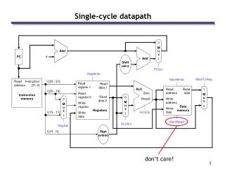
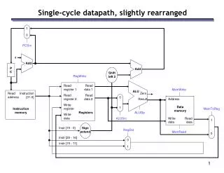
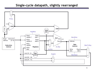
Inst Memory Adr Adder Mux Adder Putting it All Together: A Single Cycle Datapath Instruction<31:0> <21:25> <16:20> <11:15> <0:15> Rs Rt Rd Imm16 RegDst nPC_sel ALUctr MemWr MemtoReg Equal Rt Rd 3 0 1 Rs Rt 4 RegWr 5 5 5 busA Rw Ra Rb = busW 00 32 32 32-bit Registers ALU 0 32 busB 32 0 PC 32 Mux Mux Clk 32 WrEn Adr 1 Clk 1 Data In Extender Data Memory imm16 PC Ext 32 16 imm16 Clk ExtOp ALUSrc
Step 4: Given Datapath: RTL -> Control Instruction<31:0> Inst Memory <0:5> <26:31> <21:25> <16:20> <11:15> <0:15> Adr Op Fun Rt Rs Rd Imm16 Control ALUctr nPC_sel MemWr MemtoReg ALUSrc RegWr RegDst ExtOp Equal DATA PATH
Instruction<31:0> nPC_sel Instruction Fetch Unit Rd Rt <21:25> <16:20> <11:15> <0:15> Clk RegDst 1 0 Mux Rt Rs Rd Imm16 Rs Rt RegWr ALUctr 5 5 5 MemtoReg busA Zero MemWr Rw Ra Rb busW 32 32 32-bit Registers 0 ALU 32 busB 32 0 Clk Mux 32 Mux 32 1 WrEn Adr 1 Data In 32 Data Memory Extender imm16 32 16 Clk ALUSrc ExtOp A Single Cycle Datapath • We have everything except control signals (underlined) • Today’s lecture will look at how to generate the control signals
Meaning of the Control Signals • ExtOp: “zero”, “sign” • ALUsrc: 0 => regB; 1 => immed • ALUctr: “add”, “sub”, “or” • MemWr: write memory • MemtoReg: 0 => ALU; 1 => Mem • RegDst: 0 => “rt”; 1 => “rd” • RegWr: write dest register RegDst ALUctr MemWr MemtoReg Equal Rt Rd 3 0 1 Rs Rt RegWr 5 5 5 busA = Rw Ra Rb busW 32 32 32-bit Registers ALU 0 32 busB 32 0 32 Mux Mux Clk 32 WrEn Adr 1 1 Data In Extender Data Memory imm16 32 16 Clk ExtOp ALUSrc
31 26 21 16 11 6 0 op rs rt rd shamt funct 6 bits 5 bits 5 bits 5 bits 5 bits 6 bits RTL: The Add Instruction • add rd, rs, rt • mem[PC] Fetch the instruction from memory • R[rd] <- R[rs] + R[rt] The actual operation • PC <- PC + 4 Calculate the next instruction’s address
31 26 21 16 11 6 0 op rs rt rd shamt funct The Single Cycle Datapath during Add/Sub • R[rd] <- R[rs] op R[rt] Instruction<31:0> nPC_sel= +4 Instruction Fetch Unit Rd Rt <21:25> <16:20> <11:15> <0:15> Clk RegDst = 1 1 0 Mux ALUctr = Add Rt Rs Rd Imm16 Rs Rt RegWr = 1 5 5 5 MemtoReg = 0 busA Zero MemWr = 0 Rw Ra Rb busW 32 32 32-bit Registers 0 ALU 32 busB 32 0 Clk Mux 32 Mux 32 1 WrEn Adr 1 Data In 32 Data Memory Extender imm16 32 16 Clk ALUSrc = 0 ExtOp = x
Inst Memory Adr Adder Mux Adder Instruction Fetch Unit at the End of Add • PC <- PC + 4 • This is the same for all instructions except Branch and Jump Instruction<31:0> nPC_sel = +4 4 00 PC Clk imm16
31 26 21 16 0 op rs rt immediate The Single Cycle Datapath during Load • R[rt] <- Data Memory {R[rs] + SignExt[imm16]} Instruction<31:0> nPC_sel= +4 Instruction Fetch Unit Rd Rt <21:25> <16:20> <11:15> <0:15> Clk RegDst = 0 1 0 Mux ALUctr = Add Rt Rs Rd Imm16 Rs Rt RegWr = 1 MemtoReg = 1 5 5 5 busA Zero MemWr = 0 Rw Ra Rb busW 32 32 32-bit Registers 0 ALU 32 busB 32 0 Clk Mux 32 Mux 1 WrEn Adr 1 Data In 32 Data Memory Extender 32 imm16 32 16 Clk ALUSrc = 1 ExtOp = 1
31 26 21 16 0 op rs rt immediate The Single Cycle Datapath during Store • Data Memory {R[rs] + SignExt[imm16]} <- R[rt] Instruction<31:0> nPC_sel= +4 Instruction Fetch Unit Rd Rt <21:25> <16:20> <11:15> <0:15> Clk RegDst = x 1 0 Mux ALUctr = Add Rt Rs Rd Imm16 Rs Rt RegWr = 0 5 5 5 MemtoReg = x busA Zero MemWr = 1 Rw Ra Rb busW 32 32 32-bit Registers 0 ALU 32 busB 32 0 Clk Mux 32 Mux 32 1 WrEn Adr 1 32 Data In Data Memory Extender imm16 32 16 Clk ALUSrc = 1 ExtOp = 1
31 26 21 16 0 op rs rt immediate The Single Cycle Datapath during Branch • if (R[rs] - R[rt] == 0) then Zero <- 1 ; else Zero <- 0 Instruction<31:0> nPC_sel= “Br” Instruction Fetch Unit Rd Rt <21:25> <16:20> <11:15> <0:15> Clk RegDst = x 1 0 Mux ALUctr = Subtract Rt Rs Rd Imm16 Rs Rt RegWr = 0 MemtoReg = x 5 5 5 busA Zero MemWr = 0 Rw Ra Rb busW 32 32 32-bit Registers 0 ALU 32 busB 32 0 Clk Mux 32 Mux 32 1 WrEn Adr 1 Data In 32 Data Memory Extender imm16 32 16 Clk ALUSrc = 0 ExtOp = x
31 26 21 16 0 op rs rt immediate Inst Memory Adr Adder Mux Adder Instruction Fetch Unit at the End of Branch • if (Zero == 1) then PC = PC + 4 + SignExt[imm16]*4 ; else PC = PC + 4 Instruction<31:0> nPC_sel See book for what the datapath and control looks like for jump instructions. Compared to book our processor also supports the ORI instructions. 4 00 PC Clk imm16
add sub ori lw sw beq jump RegDst 1 1 0 0 x x x ALUSrc 0 0 1 1 1 0 x MemtoReg 0 0 0 1 x x x RegWrite 1 1 1 1 0 0 0 MemWrite 0 0 0 0 1 0 0 nPCsel 0 0 0 0 0 1 0 Jump 0 0 0 0 0 0 1 ExtOp x x 0 1 1 x x ALUctr<2:0> Add Subtract Or Add Add xxx Subtract 31 26 21 16 11 6 0 op rs rt rd shamt funct immediate op rs rt op target address A Summary of the Control Signals See func 10 0000 10 0010 We Don’t Care :-) Appendix A op 00 0000 00 0000 00 1101 10 0011 10 1011 00 0100 00 0010 R-type add, sub I-type ori, lw, sw, beq J-type jump
op 00 0000 00 1101 10 0011 10 1011 00 0100 00 0010 R-type ori lw sw beq jump RegDst 1 0 0 x x x ALUSrc 0 1 1 1 0 x MemtoReg 0 0 1 x x x RegWrite 1 1 1 0 0 0 MemWrite 0 0 0 1 0 0 Branch 0 0 0 0 1 0 Jump 0 0 0 0 0 1 ExtOp x 0 1 1 x x ALUop<N:0> “R-type” Or Add Add xxx Subtract ALU Control (Local) Step 5: The Concept of Local Decoding func ALUctr op 6 Main Control 3 ALUop 6 N ALU
func ALU Control (Local) op 6 ALUctr Main Control ALUop 6 3 N The Encoding of ALUop • In this exercise, ALUop has to be N=2 bits wide to represent: • (1) “R-type” instructions • “I-type” instructions that require the ALU to perform: • (2) Or, (3) Add, and (4) Subtract • To implement the full MIPS ISA, ALUop has to be 3 bits to represent: • (1) “R-type” instructions • “I-type” instructions that require the ALU to perform: • (2) Or, (3) Add, (4) Subtract (5) And (6) Set on < R-type ori lw sw beq jump ALUop (Symbolic) “R-type” Or Add Add xxx Subtract ALUop<2:0> 1 00 0 10 0 00 0 00 xxx 0 01
func ALU Control (Local) op 6 ALUctr Main Control ALUop 6 3 N R-type ori lw sw beq jump ALUop (Symbolic) “R-type” Or Add Add xxx Subtract ALUop<2:0> 1 00 0 10 0 00 0 00 xxx 0 01 31 26 21 16 11 6 0 R-type op rs rt rd shamt funct funct<5:0> Instruction Operation ALUctr<2:0> ALU Operation 10 0000 add 000 Add 10 0010 subtract 001 Subtract 10 0100 and 010 And 10 0101 or 110 Or 10 1010 set-on-less-than 111 Set-on-less-than The Decoding of the “func” Field Our processor only implements subset of operations Get func from back of book for R-type
R-type ori lw sw beq ALUop (Symbolic) “R-type” Or Add Add Subtract ALUop<2:0> 1 00 0 10 0 00 0 00 0 01 ALUop func ALU Operation ALUctr bit<2> bit<1> bit<0> bit<3> bit<2> bit<1> bit<0> bit<2> bit<1> bit<0> 0 0 0 x x x x Add 0 1 0 0 x 1 x x x x Subtract 1 1 0 0 1 x x x x x Or 0 0 1 1 x x 0 0 0 0 Add 0 1 0 1 x x 0 0 1 0 Subtract 1 1 0 1 x x 0 1 0 0 And 0 0 0 1 x x 0 1 0 1 Or 0 0 1 1 x x 1 0 1 0 Set on < 1 1 1 The Truth Table for ALUctr<2> funct<3:0> Instruction Op. 0000 add 0010 subtract 0100 and 0101 or 1010 set-on-less-than This control is for more R-type instructions than our processor, but fewer than the entire MIPS ISA.
The Logic Equation for ALUctr<2> ALUop func • ALUctr<2> = !ALUop<2> & ALUop<0> + ALUop<2> & func<1> bit<2> bit<1> bit<0> bit<3> bit<2> bit<1> bit<0> ALUctr<2> 0 x 1 x x x x 1 1 x x 0 0 1 0 1 1 x x 1 0 1 0 1
ALUop func ALU Operation ALUctr bit<2> bit<1> bit<0> bit<3> bit<2> bit<1> bit<0> bit<2> bit<1> bit<0> 0 0 0 x x x x Add 0 1 0 0 x 1 x x x x Subtract 1 1 0 0 1 x x x x x Or 0 0 1 1 x x 0 0 0 0 Add 0 1 0 1 x x 0 0 1 0 Subtract 1 1 0 1 x x 0 1 0 0 And 0 0 0 1 x x 0 1 0 1 Or 0 0 1 1 x x 1 0 1 0 Set on < 1 1 1 The Truth Table for ALUctr <1>
The Logic Equation for ALUctr<1> ALUop func • ALUctr<1> = !ALUop<2> & !ALUop<1> +ALUop<2> & func<2> bit<2> bit<1> bit<0> bit<3> bit<2> bit<1> bit<0> ALUctr<1> 0 0 0 x x x x 1 0 x 1 x x x x 1 1 x x 0 0 0 0 1 1 x x 0 0 1 0 1 1 x x 1 0 1 0 1
ALUop func ALU Operation ALUctr bit<2> bit<1> bit<0> bit<3> bit<2> bit<1> bit<0> bit<2> bit<1> bit<0> 0 0 0 x x x x Add 0 1 0 0 x 1 x x x x Subtract 1 1 0 0 1 x x x x x Or 0 0 1 1 x x 0 0 0 0 Add 0 1 0 1 x x 0 0 1 0 Subtract 1 1 0 1 x x 0 1 0 0 And 0 0 0 1 x x 0 1 0 1 Or 0 0 1 1 x x 1 0 1 0 Set on < 1 1 1 The Truth Table for ALUctr<0>
The Logic Equation for ALUctr<0> ALUop func • ALUctr<0> = !ALUop<2> & ALUop<1> + ALUop< 2> & func<2> & func<0> + ALUop<2> & func<3> bit<2> bit<1> bit<0> bit<3> bit<2> bit<1> bit<0> ALUctr<0> 0 1 x x x x x 1 1 x x 0 1 0 1 1 1 x x 1 0 1 0 1
func ALU Control (Local) 6 ALUctr ALUop 3 3 The ALU Control Block • ALUctr<2> = !ALUop<2> & ALUop<0> + ALUop<2> & func<1> • ALUctr<1> = !ALUop<2> & !ALUop<1> +ALUop<2> & func<2> • ALUctr<0> = !ALUop<2> & ALUop<1> + ALUop< 2> & func<2> & func<0> + ALUop<2> & func<3>
RegDst func ALUSrc ALUctr ALU Control (Local) op 6 Main Control : 3 6 ALUop 3 The “Truth Table” for the Main Control op 00 0000 00 1101 10 0011 10 1011 00 0100 00 0010 R-type ori lw sw beq jump RegDst 1 0 0 x x x ALUSrc 0 1 1 1 0 x MemtoReg 0 0 1 x x x RegWrite 1 1 1 0 0 0 MemWrite 0 0 0 1 0 0 Branch 0 0 0 0 1 0 Jump 0 0 0 0 0 1 ExtOp x 0 1 1 x x ALUop (Symbolic) “R-type” Or Add Add xxx Subtract ALUop <2> 1 0 0 0 x 0 ALUop <1> 0 1 0 0 x 0 ALUop <0> 0 0 0 0 x 1