High Electron Mobility Transistor (HEMT)
E N D
Presentation Transcript
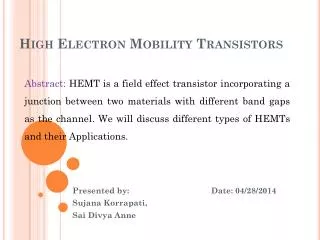
High Electron Mobility Transistor (HEMT) Flament Benjamin
PLAN • Presentation • Fabrication
Presentation • 1980 at Fujitsu • TEGFET, MODFET, HFET • Goal->transportation in a doped material
Presentation • Heterojunction: 2 layers • Highly doped layer with grand gap • Non-doped layer with small gap
PLAN • Presentation • Fabrication
Plan • Cleaning • Deposition, MBE • Ohmic contacts
Fabrication • Cleaning of the wafer • GaAs wafer->more complicated than Si wafer • Difficulties to remove the oxide of Ga and As • We use the electron cyclotron resonance (ECR)
Fabrication • As oxide is removed by heating and : x=1, 3, 5 stands for the various oxides of arsenic • Ga oxide is removed by:
Fabrication • Becomes volatile at 200°C so we choose a temperature of 400°C
Fabrication • We grow the different layer by molecular beam epitaxy (MBE)
30 periods of AlGaAs/GaAs superlattice buffer 30 periods of AlGaAs/GaAs superlattice buffer
Fabrication • 3 layers: • PPMA for the bottom layer • PMIPK for the middle layer • PPMA for the top layer • PPMA(polypropylmethacrylate) • PMIPK(polymethylisopropenylketone)
Fabrication • Using deep UV lithography
Research • Lattice matching

