Software-defined Radio using Xilinx (SoRaX)
Software-defined Radio using Xilinx (SoRaX). By: Anton Rodriguez & Mike Mensinger Advised by: Dr. In Soo Ahn & Dr. Yufeng Lu. Outline. Brief project overview/introduction Project Goals Prior work and supplements Background Dissection of Flowchart Requirements Equipment Schedule.

Software-defined Radio using Xilinx (SoRaX)
E N D
Presentation Transcript
Software-defined Radio using Xilinx(SoRaX) By: Anton Rodriguez & Mike Mensinger Advised by: Dr. In Soo Ahn & Dr. Yufeng Lu
Outline • Brief project overview/introduction • Project Goals • Prior work and supplements • Background • Dissection of Flowchart • Requirements • Equipment • Schedule
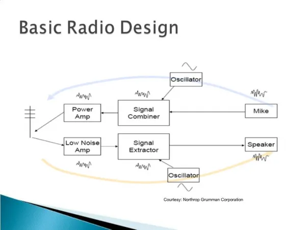
A Software-defined Radio (SDR) offers a flexible solution for many of today’s communication needs. The objective of this project is to design a communication radio system on the FPGA board. The main focus will lie on the carrier synchronization and phase ambiguity correction from the received data. We will start by designing a Simulink model of the entire system and then implement it on the SignalWave Virtex II FPGA board . Project Overview
Gain an in-depth understanding about the FPGA implementation of carrier synchronization. Construct a working Simulink model. Implement the Simulink model on the FPGA board. Regenerate the carrier and symbol timing to decode the transmitted digital data. Achieve fast acquisition of carrier synchronization and symbol timing through efficient Xilinx programming. Create a test signal of known hard-coded values (preamble) to estimate the channel state. If time permits, implement different modulation schemes (i.e. 16-QAM). Project Goals
Previous Work / Supplements • Xilinx 11.1 Example – sysgen Costas Loop • Referenced Phase-Locked Loop (PLL) Filter • FPGA Implementation of Carrier Synchronization for QAM Receivers • By Chris Dick (Xilinx, Inc.) • Previous Senior Project on QPSK receiver • With phase-locked loop • Incomplete…
Background • E E 332 QPSK Project • Wireless communication introduces distortions due to multi-paths • Need to regenerate the in-phase carrier signal
High Level Flowchart Phase-Locked Loop
Phase-Locked Loop Corrected Signal + -
Requirements • The model shall operate with a system clock of 50 MHz. • There shall be an explicit sampling period of 1/8 throughout the Simulink model. • The sampling frequency for the model should be 12.5 MHz. • We shall use the DDS compiler 2.0 to simulate our Voltage Controlled Oscillator (VCO) for the Phase-Locked Loop. • The frequency offset provided should be no larger than 1 kHz. • We shall follow the FCC Regulations for Radio Frequency Devices • Stay outside of the restricted bands of operation
Equipment • SignalWave Virtex II FPGA • Xilinx - ISE 9.2 Compiler • Virtex 4 FPGA
To this point, we have dissected all of the models we were given. Researched phase-locked loops and their components. Isolated components have been tested to be functional: Phase detector Loop filter DDS compiler Dr. Lu’s revision Progress