Layer 0 in D0 Silicon Tracker for run2b
140 likes | 159 Vues
This presentation covers the motivation, concept, and prototypes of the Layer 0 (L0) Analog Flex Cable for the D0 Silicon Tracker at Fermilab. It discusses noise and shielding studies, as well as the design goals and requirements for the cable. The presentation concludes with a summary of the progress made and prospects for future developments.

Layer 0 in D0 Silicon Tracker for run2b
E N D
Presentation Transcript
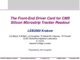
Layer 0 in D0 Silicon Tracker for run2b Kazu Hanagaki / Fermilab for D0 run2b Silicon Tracker group • Motivation & concept • Analog flex cable • Prototypes • Noise/Shielding studies • Summary and prospects Vertex 2002 Kazu Hanagaki
Motivation • Higgs search, new phenomena search, top physics, b physics… all needs b tagging. • B tagging by means of the longer life time of B meson/baryon better impact parameter resolution. measurement at position close to the decay point.s~smeas(1+Rin/Rout) • Design goal: S/N>10 after 15fb-1 for the Layer 0 (L0). • Simulation for WH(bb) events: b jet tagging efficiency 69% for run2b (50% for run2a) (0.11 for run2b, 0.27 for run2a) Vertex 2002 Kazu Hanagaki
The longest ~ 435mm The shortest ~ 243mm Concept • SVX4 chip cannot sit on the sensors because of the cooling and space issues. Signal must be read out from the sensor to the chip. Also bias voltage and its return must be provided. Low mass analog flex cable. Noise due to capacitive load and pick-up must be addressed. Vertex 2002 Kazu Hanagaki
Requirement to Analog Cable Total noise estimates VS total capacitance (Csi + Ccable) S/N=10 CSi Ccable S/N=10 after 15fb-1 Ccable < 23pF for 43.5cm long cable Ccable < 0.53pF/cm Vertex 2002 Kazu Hanagaki
Analog Cable Design FE calculation by ANSYS 50 mm pitch 100 mm pitch • 91mm trace pitch. • 16mm trace width. • No fan-in/out region. • Two cables laminated at the edges with 45mm offset. • 50 mm thick polyimide (Kapton type) substrate. 16 mm wide trace with ~100mm pitch satisfies the requirement of <0.53pF/cm • Alternative for 50mm pitch readout 50mm + 100mm + 50mm pitch Use technically simpler solution which maintains low capacitance. Vertex 2002 Kazu Hanagaki
Analog Cable Design (cont’d) 100mm pitch 8 x 16mm traces 200mm • 200 mm is enough to avoid significant contribution from other cables. • Low er material for spacer. polypropylene mesh. C = 0.328 pF/cm Contribution from: Two neighbors = 0.208 pF/cm Two top neighbors = 0.014 pF/cm Two bottom neighbors = 0.017 pF/cm 50mm Vertex 2002 Kazu Hanagaki
Prototype Cable by Dyconex • visual inspection on cables: • look for not gold-plated (copper) pads as evidence for an open trace • 129 tracesone open is allowed. • check trace width on cables: 9-12 mm depending on cable. Capacitance (one to neighbors) ~ 0.35pF/cm. Vertex 2002 Kazu Hanagaki
Fixture inside shielding w/ GND Connected to sensor/cable No connection Noise increase due to capacitive load L0 Prototype for noise studies HV • Dyconex analog cable + ELMA prototype sensor + SVX2 chip (for run2a) • Noise increase ~ 1000 e consistent with SVX2 noise performance. GND Vertex 2002 Kazu Hanagaki
Shielding • RF pick-up by the analog cable. • No external but shielding (= aluminum foil) only around the analogcable. total noise random noise Shielding metal connected to GND analog cable center region sensor SVX2 shielding length edge region edge center different shielding length Noise level w/ ext. shielding Vertex 2002 Kazu Hanagaki
Shielding (cont’d) • Must be careful about capacitive coupling to nearby floating metal. • Clear even-odd effect indicates capacitive coupling to the analog cable. Distance between the traces to the metal; top-metal ~ 100mm, bottom-metal ~ 50mm. metal piece under the cable w/o ground connection metal piece Vertex 2002 Kazu Hanagaki
L0 Prototype with SVX4 • First prototype using new SVX4 chip. • Large capacitive load • Long analog cable signal transmission • L1 prototype hybrid with SVX4. Vertex 2002 Kazu Hanagaki
Prototype w/ SVX4 (cont’d) • Successfully reads out! First time for SVX4 through long analog cable. • (Systematic noise studies not yet done…) Vertex 2002 Kazu Hanagaki
sensor HV low-pass filter board Al foil for HV Al foil for GND Kapton sheet for insulation CF fixture Grounding • Carbon Fiber (CF) support structure is regarded as a conductor for high frequency. talk by B. Quinn • Sensor ground will be tied together to the CF structure. (Only L0. The others at hybrid.) Vertex 2002 Kazu Hanagaki
Summary & Prospects • Established baseline design for the analog cable. • Test results of prototype analog cable are encouraging. • L0 prototype addresses the feasibility of our baseline design. • Noise studies are in progress. • Grounding scheme will be tested by having prototype module. Vertex 2002 Kazu Hanagaki
