High Throughput Zero Mode Waveguides via Natural Lithography
20 likes | 226 Vues
High Throughput Zero Mode Waveguides via Natural Lithography Shawn H. Pfeil , Yale E. Goldman, NSEC DMR 0832802.

High Throughput Zero Mode Waveguides via Natural Lithography
E N D
Presentation Transcript
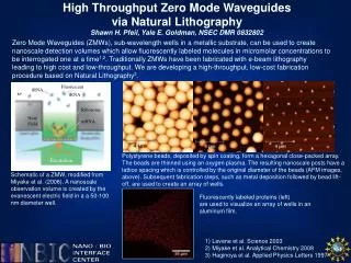
High Throughput Zero Mode Waveguides via Natural Lithography Shawn H. Pfeil, Yale E. Goldman, NSEC DMR 0832802 Zero Mode Waveguides (ZMWs), sub-wavelength wells in a metallic substrate, can be used to create nanoscale detection volumes which allow fluorescently labeled molecules in micromolar concentrations to be interrogated one at a time1,2. Traditionally ZMWs have been fabricated with e-beam lithography leading to high cost and low-throughput. We are developing a high-throughput, low-cost fabrication procedure based on Natural Lithography3. Polystyrene beads, deposited by spin coating, form a hexagonal close-packed array. The beads are thinned using an oxygen plasma. The resulting nanoscale posts have a lattice spacing which is controlled by the original diameter of the beads (AFM images, above). Subsequent fabrication steps, such as metal deposition followed by bead lift-off, are used to create an array of wells. Schematic of a ZMW, modified from Miyake et al. (2008). A nanoscale observation volume is created by the evanescent electric field in a a 50-100 nm diameter well. Fluorescently labeled proteins (left) are used to visualize an array of wells in an aluminum film. 1) Levene et al. Science 2003 2) Miyake et al. Analytical Chemistry 2008 3) Haginoya et al. Applied Physics Letters 1997