Download

1 / 1
10 likes | 149 Vues
Depth Profiling of Thin Films by Ion Beams: Formation of Nanostructures at the Interface. D. Karpuzov 1 , M. Stepanova 2 , and S. K. Dew 2 1 Alberta Centre for Surface Engineering and Science, University of Alberta, Edmonton, AB, T6G 2G6

E N D
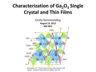
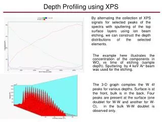
Depth Profiling of Thin Films by Ion Beams: Formation of Nanostructures at the Interface D. Karpuzov1, M. Stepanova2, and S. K. Dew2 1 Alberta Centre for Surface Engineering and Science, University of Alberta, Edmonton, AB, T6G 2G6 2 Electrical & Computer Engineering, ECERF, University of Alberta, Edmonton, AB, T6G 2V4 interface interface Cu surface Si O C 4E. Origin of fuzzy Cu patterns 4. Results and Discussion 4D. Synergistic simulation of sputtering and coarsening 4B. Surface patterns from SEM 1. Introduction 4A. Depth Profiles Well separated clusters exist only at temperatures T<<TC. When the temperature approaches the critical temperature TC, the pattern becomes fuzzy and decomposes. TC is defined from Tc=AJ/k, where the coefficient A=1.5 is found numerically [6]. For the bond energy J we used value of 0.05 eV per bond [7]. When ion energy increases, atomic mixing occurs near the interface of metal clusters and the substrate. The binding energy of cluster atoms decreases, and so does the critical temperature TC. As a result, high energy bombardment leads to fuzzy degraded patterns. Cu on Si : Copper films on Si sputtered by 1 keV Ar ions evolve in percolative networks with characteristic feature size of ~100nm. With continuing sputtering, the network shrinks into elongated Cu clusters. The ion energies of 3 keV and higher lead to fuzzy patterns, see the 5 keV pattern in Fig. 3. • Ion bombardment is routinely used in ion-beam assisted deposition of thin films as well as an etching tool in surface analysis techniques. • Gradual erosion of the top layers is usually assumed. • Surface topography changes such as ripples and cones were found earlier for high-energy ion bombardment of bulk solids [1]. Submicron patterns of thin films etched at 100 keV and substrate temperature of 200-400 oC were also observed [2]. • No data are reported sofar for RT ion etching of thin films. • We have performed numerical simulations combining surface diffusion and sputtering. • Surface diffusion proceeds through jumps of adatoms. Considered are individual adatoms and 1ML terraces at cluster edges (Fig. 5) • Sputtering is accounted for by the removal of single adatoms and adatoms located at cluster periphery (Fig.5). Fig. 7. Simulated fuzzy pattern at T=0.7TC Fig.3. Surface patterns at Cu/Si interfaces developed under 1 keV Ar ion bombardment (left), 3 keV (middle) and 5 keV (right). Angle of incidence is 45o. Fig.5. The model of clusters in our simulation: 1ML perimeter that is subject to diffusion (left) and shrinkage of clusters by sputtering (right). Fig. 1. XPS Cu 2p peaks at various depth, surface at the back and interface at the front. Etching by 1 keV Ar+ beam, 45o incidence. Note the metallic character of the bond. 5. Conclusions 2. Experimental • Sputtering of Cu/Si and Ag/Si interfaces by keV-energy ions at RT results in formation of ~100nm sized metal networks and clusters. • Cu/Si interfaces develop well-defined patterns when bombarded with 1 keV ions, whereas bombardment with 3 keV and higher ion energies leads to fuzzy patterns. • The features observed for Ag are 3-4 times larger than similar features for Cu. • The observed trends can be explained by an interplay of ion-induced sputtering and coarsening of surface patterns. • Cluster formation can affect the depth profiling by ion beam sputtering, used in most surface analysis instruments. The resulting simulated pattern has a maximum size λmax The size λmax is an increasing function of the parameter D/JY , where D is the diffusivity of adatoms, Y is the sputtering yield, J is the ion flux. This predicts λmax.(Ag) > λmax.(Cu), in agreement with the experiment. . Ag on Si : Silver films on Si sputtered by 3 keV Ar ions develop networks similar to those observed for Cu, but the characteristic size is larger, ~300 nm (Fig.4). With continuing sputtering, the networks shrink into separate Ag clusters. Copper and silver thin films (15 – 50 nm) were deposited on Si substrates by magnetron sputtering at RT. The deposited films were etched by an Ar ion beam in an XPS spectrometer (AXIS 165, Kratos). Ion beam energy ranged between 1 and 5 keV and the incident angle was 45°. Ion etching was halted near the interface and the surface composition was assessed by XPS. The samples were removed from the vacuum chamber and analyzed by SEM (Jeol, 6301FXV) Fig. 1a. Depth profile of composition, Cu/Si. Bombardment conditions as in Fig. 1a. Initially sharp interface appears as a gradual change of concentrations Fig. 4. SEM patterns at Ag/Si interfaces. With increased time of sputtering (from left to right) the network evolves into separate clusters. Acknowledgements M.S and S.K.D are grateful to NSERC and iCORE for support. D.S.K acknowledges the CFI and ASRA grants. 3. Simulation Models 4C. Interpretation References • Ion beam depth profiling was investigated by dynamic Monte-Carlo simulation of ion and recoil trajectories taking into account surface erosion and composition changes [3]. • To investigate self-assembled patterns on the surface, an original Monte-Carlo simulation was developed [4]. The simulation uses a 2D lattice partially covered by adatoms. The model includes removal of adatoms from favored positions by sputtering and surface diffusion. [1] G.Carter, J.Phys. D34, R1 (2001); U. Valbusa, C. Bogarno, and F. Buatier de Mongeot, J. Phys: Condens. Matter. 14 8153 (2002). [2] D.K.Sakar, S.Dhara, K.G.M.Nair, and S.Chowdhury, Nucl. Instrum. Meth. B170, 413 (2000). [3] I.R.Chakarov, S.S.Todorov and D.S.Karpuzov: Nucl.Instrum.Meth. B69, 193 (1992). [4] M. Stepanova, S. K. Dew, and D. S. Karpuzov, in preparation. [5] M.Zinke-Allmang, L.C.Feldman, and M.H.Grabow, Surf.Sci. Rep. 16, 377 (1992). [6] K. Binder and D.W.Heerman, “Monte Carlo Simulation in Statistical Physics”, Springer, 1988. [7] M. Giesen, Progr. In Surf.. Sci. 68, 1 (2001) • The observed patterns can be explained by an interplay of sputtering and a coarsening process known as Ostwald ripening [5]: • Initially, a network is formed as a result of of variations in the metal film thickness. • In the course of ion bombardment, Ostwald ripening increases the size of network features whereas sputtering makes them shrink. • The observed size of features is defined by relative rates of coarsening and sputtering. Fig. 1b. Same as Fig. 1b, comparison of etching at 1 keV (left) and 5 keV (right) Fig. 6. Simulated feature size as a function of the number of MC jump steps, n, for T=0.3TC. Scaling for L×L lattice: n0= 1.56·10-2L3 MC steps/cell, S=(number of MC sputter steps)/n =6.25·10-11L2 Fig. 1c. Copper concentration at the surface simulated by DYNTRIM, 1 keV (left) 3 keV (middle), and 5 keV (right).