Download
1 / 25
260 likes | 396 Vues
X-rays techniques as a powerful tool for characterisation of thin film nanostructures El ż bieta Dynowska. Institute of Physics Polish Academy of Sciences, al. Lotników 32/46, Warsaw, Poland dynow@ifpan.edu.pl.

E N D
X-rays techniques as a powerful tool for characterisation of thin film nanostructures Elżbieta Dynowska Institute of Physics Polish Academy of Sciences, al. Lotników 32/46, Warsaw, Poland dynow@ifpan.edu.pl Workshop on Semiconductor Processing for Photonic Devices, Sept. 30 – Oct. 2, Warsaw, Poland
Outline 1. Introduction 2. Basics General information about nanostructures What we want to know about thin layers? How to get this information? 3. Selected X-ray techniques X-ray reflectivity X-ray diffraction 4. Synchrotron radiation – new possibilities 5. Summary
Thin layer – the dimension in the z-direction is much smaller than in the x and y, respectively. z y 0 z y x 0 single crystal thin layer having the crystal structure and orientation of single crystal substrate on which it was grown. (A) Epitaxial layer x Homoepitaxial layer – the layer and substrate are the same material (the same lattice parameters). Heteroepitaxial layer – the layer material is different than the substrate one (different lattice parameters).
az ay ax as alayer Lattice mismatch – f = (alayer - asubs )/ asubs Critical thickness hc – thickness below which the layer grows pseudomorphicallythe cubic unit cell of layer material is tetragonally distorted: alz alx= aly= as (the layer is fully strained). hcdecreasing when fincreasing. Layer relaxation - alxy alz al relax= abulk (B) Polycrystalline layers – orientations of small crystallites are randomly distributed with respect to layer surface (C) Amorphous layers - lack of long-distance ordering of atoms
What we want to know about thin layers? Crystalline state of layer/layers (epitaxial?; polycrystalline?; amorphous? …) crystal quality; strain state; defect structure; chemical composition (in the case of ternary compounds layers); thickness surface and interface roughness, and so on…
How to get this information? By means of X-ray techniques Why? Because X-ray techniques are the most important, non-destructive methods of samplecharacterization
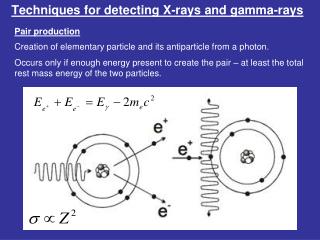
kR kI c kT i i i t Selected X-ray techniques X-ray reflectivitySmall-angle region Refraction index for X-rays n < 1: Roughness investigation n = 1- + i ~10-5 in solid materials (~10-8 in air); - usually much smaller than . z 2i x Si rough wafer - simulation Layer thickness determination The distance between the adjacent interference maxima can be approximated by: i / 2t
Si cap-layer Fe2N Fe GaAs Example: superlattice Si/{Fe/Fe2N}x28/GaAs(001) Results of simulation Experiment Simulation 10.4 nm Intensity (2) -superlattice period 126.6nm 28 times repeated All superlattice 4.52nm (2) – cap-layer c0.3 i (deg)
d’hkl X-ray diffraction wide-angle region Bragg’s law: n = 2d’sin d’/n = d = 2d sin
Detector Incident beam Diffracted beam 2 ’ Detector Incident beam Diffracted beam 2 Geometry of measurement /2 coupling /2 coupling
Possibilities Crystalline state of layer/phase analysis MnTe/Al2O3 ZnMnTe/MnTe/Al2O3 CuK1 radiation FeK radiation
Crystal quality „Rocking curve” Detector 21 arcsec 112 arcsec Lattice parameter fluctuations ? Mosaic structure
az ay ax as alayer Strain state & defect structure Strain tetragonal deformation of cubic unit cell: Pseudomorphic case Cubic unit cell of layer material az ax = ay = asub az Partially relaxed ay ax Cubic unit cell of substrate: az ax =ayasub alayer Relaxed az = ax = ay = alayer
004 003 002 102 202 001 101 201 Origin 100 200 300 P = [001] sample Lattice parameter fluctuations relaxed The reciprocal lattice maps Reciprocal lattice: The sample orientation can be described by two vectors: P - vector which is the direction normal to the sample surface; S – any other vector which is not parallel to the P vector and lies in the horizontal plane. |H|102 = 1/d102 S = [100] pseudomorphic Mosaic structure
Examples z x d00l dhhl dz dx In0.50Al0.50As/InP 004 004 Symmetric case (a) (b) 224 224 Asymmetric case For cubic system: For tetragonal system:
abulk aACB x 0 x 1 chemical composition If AB and CB compounds having the same crystallographic system and space group create the ternary compound A1-xCxBthen its lattice parameter a ACB depends linearly on x-value between the lattice parameters values of AB and CB, respectively. Vegard’s rule: In the case of thin layers arelaxed must be taken for chemical composition determination from Vegard’s rule: aCB aAB c12, c11 – elastic constants of layer material
Heterostructure: ZnMnxTe/ZnMnyTe/ZnMnzTe/ZnTe/GaAs 004 rocking curve ZnTe 004 x y z 004 /2 335 relaxed pseudomorphic
Towards an ohmic contacts Ti/TiN/GaN/Al2O3 under annealing Secondary Ion Mass Spectrometry (SIMS) XRD
NbN/GaN/Al2O3 (SIMS) XRD (SIMS) XRD
Deposition of Zn3N2 by reactive rf sputtering GaN, Al2O3, ZnO Zn3N2 20% N2 Zn3N2 + Zn 25% N2 polycryst. Zn3N2 N2>80% polycryst. & amorph. 50% - 70% N2 monocryst.
polycrystalline ZnO on sapphire and quartz ZnO:N by oxidation of Zn3N2 microstructure highly textured ZnO on GaN and ZnO
ZnO by oxidation of ZnTe/GaAs XRD (SIMS) Te inclusions in ZnO film
Si, 24 nm, 450 C Si, 10 nm, 480 C Si, 115 nm, 780 C Si substrate (001) Example:superlattice of self-assembled ultra-small Ge quantum dots Results:HREM XRD superlattice period C..... 33.5 nm 33 nm, thickness of Ge............... 1.8 nm 2.0 nm thickness of SiGex bottom layer..................... 6.7 nm 6.7 nm Compositon........................ ---- x 0.2 7 times repeated C Si, 2nm, 250 C Ge, 1nm, 250 C 50nm High resolution electron microscopy (HREM) – JEOL-4000EX (400 keV) Hasylab (Hamburg), W1.1 beamline: X’Pert Epitaxy and Smoothfit software Si 004 Ge 004 2 = 0.314o „-1” „-2” Si0.8Ge0.2 bottom layer Experimental diffraction pattern Simulated diffraction pattern
Acknowledgements I would like to express my gratitude to my colleagues for their kind help: Eliana Kaminska Jarek Domagala Roman Minikayev Artem Shalimov