Conductivity
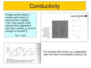
Conductivity. Charge carriers follow a random path unless an external field is applied. Then, they acquire a drift velocity that is dependent upon their mobility, m n and the strength of the field, x V d = - m n x. The average drift velocity, v av is dependent

Conductivity
E N D
Presentation Transcript
Conductivity Charge carriers follow a random path unless an external field is applied. Then, they acquire a drift velocity that is dependent upon their mobility,mnand the strength of the field,x Vd = -mnx The average drift velocity, vav is dependent Upon the mean time between collisions, 2t
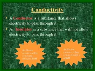
Charge Flow and Current Density Current density, J, is the rate at which charges, cross any plane perpendicular to the flow direction. J = -nqvd = nqmnx = sx n is the number of charges, and q is the charge (1.6 x 10⁻¹⁹ C) The total current density depends upon the total charge carriers, which can be ions, electrons, or holesJ = q(nmn + pmp) x OHM’s Law: V = IR Resistance, R(W) is an extrinsic quantity. Resistivity, r(Wm), is the corresponding intrinsic property. r = R*A/l Conductivity, s, is the reciprocal of resistivity: s(Wm)-1 = 1/r
CONDUCTIVITY: COMPARISON -1 • Room T values (Ohm-m) 4
As the distance between atoms decreases, the energy of each orbital must split, since according to Quantum Mechanics we cannot have two orbitals with the same energy. The splitting results in “bands” of electrons. The energy difference between the conduction and valence bands is the “gap energy” We must supply this much energy to elevate an electron from the valence band to the conduction band. If Eg is < 2eV, the material is a semiconductor.
Simple representation of silicon atoms bonded in a crystal. The dotted areas are covalent or shared electron bonds. The electronic structure of a single Si atom is shown conceptually on the right. The four outermost electrons are the valence electrons that participate in covalent bonds. Electron (-) and hold (+) pair generation represented b a broken bond in the crystal. Both carriers are mobile and can carry current. Portion of the periodic table relevant to semiconductor materials and doping. Elemental semiconductors are in column IV. Compound semiconductors are combinations of elements from columns III and V, or II and VI.
Simple band and bond representations of pure silicon. Bonded electrons lie at energy levels below Ev; free electrons are above Ec. The process of intrinsic carrier generation is illustrated in each model. Simple band and bond representations of doped silicon. EA and ED represent acceptor and donor energy levels, respectively. P- and N-type doping are illustrated in each model, using As as the donor and B as the acceptor
CONDUCTION & ELECTRON TRANSPORT • Metals: -- Thermal energy puts many electrons into a higher energy state. • Energy States: -- the cases below for metals show that nearby energy states are accessible by thermal fluctuations. 6
ENERGY STATES: INSULATORS AND SEMICONDUCTORS • Semiconductors: --Higher energy states separated by a smaller gap. • Insulators: --Higher energy states not accessible due to gap. 7
METALS: RESISTIVITY VS T, IMPURITIES • Imperfections increase resistivity --grain boundaries --dislocations --impurity atoms --vacancies These act to scatter electrons so that they take a less direct path. • Resistivity increases with: --temperature --wt% impurity --%CW 8
PURE SEMICONDUCTORS: CONDUCTIVITY VS T • Data for Pure Silicon: --s increases with T --opposite to metals electrons can cross gap at higher T material Si Ge GaP CdS band gap (eV) 1.11 0.67 2.25 2.40 10
CONDUCTION IN TERMS OF ELECTRON AND HOLE MIGRATION • Concept of electrons and holes: Adapted from Fig. 18.10, Callister 6e. • Electrical Conductivity given by: 3 # holes/m hole mobility 3 electron mobility # electrons/m 11
INTRINSIC VS EXTRINSIC CONDUCTION • Intrinsic: # electrons = # holes (n = p) --case for pure Si • Extrinsic: --n ≠ p --occurs when impurities are added with a different # valence electrons than the host (e.g., Si atoms) • N-type Extrinsic: (n >> p) • P-type Extrinsic: (p >> n) 12
Behavior of free carrier concentration versus temperature. Arsenic in silicon is qualitatively illustrated as a specific example (ND = 1015 cm-3). Note that at high temperatures ni becomes larger than 1015 doping and n≈ni. Devices are normally operated where n= ND+. Fabrication occurs as temperatures where n≈ni Probability of an electron occupying a state. Fermi energy represents the energy at which the probability of occupancy is exactly ½. Fermi level position in an undoped (left), N-type (center) and P-type (right) semiconductor. The dots represent free electrons, the open circles represent mobile holes.
Fermi-Dirac statistics Conductivity in semiconductors is described by Fermi-Dirac statistics. In general, for both extrinsic and intrinsic, the conductivity formula is: n-type: DE = Ec-Ed , n=1 P-type: DE = Ea-Ev , n=1 Intrinsic: DE = Eg, n=2
DOPED SEMICONDUCTOR: CONDUCTIVITY VS T • Data for Doped Silicon: --s increases doping --reason: imperfection sites lower the activation energy to produce mobile electrons. • Comparison:intrinsic vs extrinsic conduction... --extrinsic doping level: 1021/m3 of a n-type donor impurity (such as P). --for T < 100K: "freeze-out" thermal energy insufficient to excite electrons. --for 150K < T < 450K: "extrinsic" --for T >> 450K: "intrinsic" 13
P-N RECTIFYING JUNCTION • Allows flow of electrons in one direction only (e.g., useful to convert alternating current to direct current. • Processing: diffuse P into one side of a B-doped crystal. • Results: --No applied potential: no net current flow. --Forward bias: carrier flow through p-type and n-type regions; holes and electrons recombine at p-n junction; current flows. --Reverse bias: carrier flow away from p-n junction; carrier conc. greatly reduced at junction; little current flow. 14