Conductivity
Conductivity. Electrical conductivity Energy bands in solids Band structure and conductivity Semiconductors Intrinsic semiconductors Doped semiconductors n-type materials p-type materials Diodes and transistors p-n junction depletion region forward biased p-n junction

Conductivity
E N D
Presentation Transcript
Conductivity • Electrical conductivity • Energy bands in solids • Band structure and conductivity • Semiconductors • Intrinsic semiconductors • Doped semiconductors • n-type materials • p-type materials • Diodes and transistors • p-n junction • depletion region • forward biased p-n junction • reverse biased p-n junction • diode • bipolar transistor • operation of bipolar pnp transistor • FET • Superconductivity • Hall effect – lab experiment
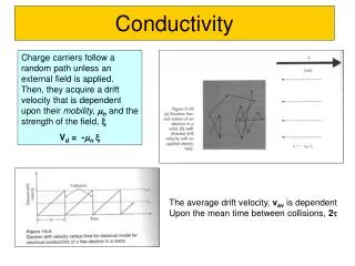
ELECTRICAL CONDUCTIVITY • in order of conductivity: superconductors, conductors, semiconductors, insulators • conductors: material capable of carrying electric current, i.e. material which has “mobile charge carriers” (e.g. electrons, ions,..) e.g. metals, liquids with ions (water, molten ionic compounds), plasma • insulators: materials with no or very few free charge carriers; e.g. quartz, most covalent and ionic solids, plastics • semiconductors: materials with conductivity between that of conductors and insulators; e.g. germanium Ge, silicon Si, GaAs, GaP, InP • superconductors: materials with zero resistivity at very low temperature
resistivities • some representative resistivities (): • R = L/A, R = resistance, L = length, A = cross section area; resistivity at 20o C • resistance(in ) (L=1m, diam =1mm) resistivity in m • aluminum 2.8x10⁻⁸ 3.6x10⁻² • brass 8x10⁻⁸ 10.1x10⁻² • copper 1.7x10⁻⁸ 2.2x10⁻² • platinum 10x10-8 12.7x10⁻² • silver 1.6x10⁻⁸ 2.1x10⁻² • carbon 3.5x10⁻⁵ 44.5 • germanium 0.45 5.7x10⁵ • silicon 640 6x10⁸ • porcelain 1010 - 1012 1016 - 1018 • teflon 1014 1020 • blood 1.5 1.9x10⁶ • fat 24 3x10⁷
ENERGY BANDS IN SOLIDS: • In solid materials, electron energy levels form bands of allowed energies, separated by forbidden bands • valence band = outermost (highest) band filled with electrons (“filled” = all states occupied) • conduction band = next highest band to valence band (empty or partly filled) • “gap” = energy difference between valence and conduction bands, = width of the forbidden band • Note: • electrons in a completely filled band cannot move, since all states occupied (Pauli principle); only way to move would be to “jump” into next higher band - needs energy; • electrons in partly filled band can move, since there are free states to move to. • Classification of solids into three types, according to their band structure: • insulators: gap = forbidden region between highest filled band (valence band) and lowest empty or partly filled band (conduction band) is very wide, about 3 to 6 eV; • semiconductors: gap is small - about 0.1 to 1 eV; • conductors: valence band only partially filled, or (if it is filled), the next allowed empty band overlaps with it
INTRINSIC SEMICONDUCTORS • semiconductor = material for which gap between valence band and conduction band is small; (gap width in Si is 1.1 eV, in Ge 0.7 eV). • at T = 0, there are no electrons in the conduction band, and the semiconductor does not conduct (lack of free charge carriers); • at T > 0, some fraction of electrons have sufficient thermal kinetic energy to overcome the gap and jump to the conduction band; fraction rises with temperature; e.g. density of conduction electrons in Si: ≈ 0.9x10¹⁰/cm3 at 20o C (293 K); ≈ 7.4x10¹⁰/cm3 at 50o C (323 K). • electrons moving to conduction band leave “hole” (covalent bond with missing electron) behind; under influence of applied electric field, neighboring electrons can jump into the hole, thus creating a new hole, etc. holes can move under the influence of an applied electric field, just like electrons; both contribute to conduction. • in pure Si and Ge: nb. of holes (“p-type charge carriers”) = nb. of conduction electrons (“n-type charge carriers”); • pure semiconductors also called “intrinsic semiconductors”.
Intrinsic silicon: • DOPED SEMICONDUCTORS: • “doped semiconductor”: (also “impure”, “extrinsic”) = semiconductor with small admixture of trivalent or pentavalent atoms;
n-type material • donor (n-type) impurities: • dopant with 5 valence electrons (e.g. P, As, Sb) • 4 electrons used for covalent bonds with surrounding Si atoms, one electron “left over”; • left over electron is only loosely bound only small amount of energy needed to lift it into conduction band (0.05 eV in Si) • “n-type semiconductor” has conduction electrons, very few holes (just the few intrinsic holes) • example: doping fraction of 10-8 Sb in Si yields about 5x10¹⁶ conduction electrons per cubic centimeter at room temperature, i.e. gain of 5x10⁶ over intrinsic Si.
p-type material • acceptor (p-type) impurities: • dopant with 3 valence electrons (e.g. B, Al, Ga, In) only 3 of the 4 covalent bonds filled vacancy in the fourth covalent bond hole • “p-type semiconductor” has mobile holes, very few mobile electrons (only the intrinsic ones). • advantages of doped semiconductors: • can”tune” conductivity by choice of doping fraction • can choose “majority carrier” (electron or hole) • can vary doping fraction and/or majority carrier within piece of semiconductor • can make “p-n junctions” (diodes) and “transistors”
n – type material p– type material
Majority and Minority Carriers • n-type material: • majority carrier: electrons • minority carrier: holes • p-type material: • majority carrier: holes • minority carrier: electrons
DIODES AND TRANSISTORS • p-n JUNCTION: • p-n junction = semiconductor in which impurity changes abruptly from p-type to n-type ; • “diffusion” = movement due to difference in concentration, from higher to lower concentration; • in absence of electric field across the junction, holes “diffuse” towards and across boundary into n-type and capture electrons; • electrons diffuse across boundary, fall into holes (“recombination of majority carriers”); formation of a “depletion region” (= region without free charge carriers) around the boundary; • charged ions are left behind (cannot move): • negative ions left on p-side net negative charge on p-side of the junction • positive ions left on n-side net positive charge on n-side of the junction • electric field across junction which prevents further diffusion.
p-n junction • Formation of depletion region in p-n junction:
DIODE • diode = “biased p-n junction”, i.e. p-n junction with voltage applied across it • “forward biased”: p-side more positive than n-side; • “reverse biased”: n-side more positive than p-side; • forward biased diode: • the direction of the electric field is from p-side towards n-side • p-type charge carriers (positive holes) in p-side are pushed towards and across the p-n boundary, • n-type carriers (negative electrons) in n-side are pushed towards and across n-p boundary current flows across p-n boundary
Forward biased pn-junction • Depletion region and potential barrier reduced
Reverse biased diode • reverse biased diode: applied voltage makes n-side more positive than p-side electric field direction is from n-side towards p-side pushes charge carriers away from the p-n boundary depletion region widens, and no current flows • diode conducts only when positive voltage applied to p-side and negative voltage to n-side • diodes used in “rectifiers”, to convert ac voltage to dc.
Reverse biased diode • Depletion region becomes wider, barrier potential higher
TRANSISTORS • (bipolar) transistor = combination of two diodes that share middle portion, called “base” of transistor; other two sections: “emitter'' and “collector”; • usually, base is very thin and lightly doped. • two kinds of bipolar transistors: pnp and npn transistors • “pnp” means emitter is p-type, base is n-type, and collector is p-type material; • in “normal operation of pnp transistor, apply positive voltage to emitter, negative voltage to collector;
operation of pnp transistor: • if emitter-base junction is forward biased, “holes flow” from battery into emitter, move into base; • some holes annihilate with electrons in n-type base, but base thin and lightly doped most holes make it through base into collector, • holes move through collector into negative terminal of battery; i.e. “collector current” flows whose size depends on how many holes have been captured by electrons in the base;
Transistor operation • Number of holes captured depends on the number of n-type carriers in the base • Number of n-type carriers can be controlled by the size of the current (the “base current”) that is allowed to flow from the base to the emitter; • base current is usually very small; • small changes in the base current can cause a big difference in the collector current; • transistor acts as amplifier of base current, since small changes in base current cause big changes in collector current. • transistor as switch: if voltage applied to base is such that emitter-base junction is reverse-biased, no current flows through transistor -- transistor is “off” • therefore, a transistor can be used as a voltage-controlled switch; computers use transistors in this way.
Field-effect transistor (FET) • In FETs, current through “channel” from “source” to “drain” is controlled by voltage (electric field) applied to the “gate” • in a pnp FET, current flowing through a thin channel of n-type material is controlled by the voltage (electric field) applied to two pieces of p-type material (“gate”) on either side of the channel (current depends on electric field). • Advantage of FET over bipolar transistor: very small gate current – small power consumption • Many different kinds of FETs • FETs are the kind of transistor most commonly used in computers.
LEDs • “Forward biased” pn junction – diode: • “forward biased”, i.e. p-side +, n-side – • current flows charge-carriers (electrons and electron holes) flow into the junction from the electrodes • electron meets a hole falls into a lower energy level releases energy in the form of a photon (light) • wavelength of emitted light depends on the materials used to make the diode (h = gap energy)
LEDs • Red: aluminum gallium arsenide (AlGaAs). • Blue: indium gallium nitride (InGaN) • green: aluminum gallium phosphide (AlGaP) • "White" light by combining light from red, green, and blue (RGB) LEDs, or by coating a blue LED with yellow phosphor.
SUPERCONDUCTIVITY • mobile electrons in conductor move through lattice of atoms or ions that vibrate (thermal motion) • cool down conductor less vibration “easier” for electrons to get through resistivity of conductors decreases (i.e. they become better conductors) when they are cooled down • in some materials, resistivity goes to zero below a certain “critical temperature” TC • these materials called superconductors -- critical temperature TC different for different materials; • no electrical resistance electric current, once started, flows forever! • superconductivity first observed by Heike Kamerlingh Onnes (1911) in Hg (mercury) at temperatures below 4.12 K.
Superconductors • many other superconductors with critical temperatures below about 20K found by 1970 -- “high TC superconductors”: (Karl Alex Müller and Johannes Georg Bednorz, 1986) • certain ceramic oxides show superconductivity at much higher temperatures; since then many new superconductors discovered, with TC up to 125K. • advantage of high TC superconductors: • can cool with (common and cheap) liquid nitrogen rather than with (rare and expensive) liquid helium; • much easier to reach and maintain LN temperatures (77 K) than liquid Helium temperatures (few K).
Properties of superconductors • electrical resistivity is zero (currents flowing in superconductors without attenuation for more than a year) • there can be no magnetic field inside a superconductor (superconductors ”expel” magnetic field -- “Meissner effect”) • transition to superconductivity is a phase transition (without latent heat). • about 25 elements and many hundreds of alloys and compounds have been found to be superconducting • examples: In, Sn, V, Mo, Nb-Zr, Nb-Ge, Nb-Ti alloys
applications of superconductors • superconducting magnets: • magnetic fields stronger, the bigger the current - “conventional” magnets need lots of power and lots of water for cooling of the coils; • s.c. magnets use much less power (no power needed to keep current flowing, power only needed for cooling) • most common coil material is NbTi alloy; liquid He for cooling • e.g. particle accelerator “Tevatron” at Fermi National Accelerator Laboratory (“Fermilab”) uses 990 superconducting magnets in a ring with circumference of 6 km, magnetic field is 4.5 Tesla. • magnetic resonance imaging (MRI): • create images of human body to detect tumors, etc.; • need uniform magnetic field over area big enough to cover person; • can be done with conventional magnets, but s.c. magnets better suited - hundreds in use • magnetic levitation - high speed trains??
explanation of superconductivity -- 1 • Cooper pairs: • interaction of the electrons with the lattice (ions) of the material, small net effective attraction between the electrons; (presence of one electron leads to lattice distortion, second electron attracted by displaced ions) • this leads to formation of “bound pairs” of electrons (called Cooper pairs); (energy of pairing very weak - thermal agitation can throw them apart, but if temperature low enough, they stay paired) • electrons making up Cooper pair have momentum and spin opposite to each other; net spin = 0 behave like ”bosons”.
explanation of superconductivity -- 2 • unlike electrons, bosons “like” to be in the same state; when there are many of them in a given state, others also go to the same state • nearly all of the pairs locked down in a new collective ground state; this ground state is separated from excited states by an energy gap; • consequence is that all pairs of electrons move together (collectively) in the same state; electron cannot be scattered out of the regular flow because of the tendency of Bose particles to go in the same state no resistance • (explanation given by John Bardeen, Leon N. Cooper, J. Robert Schrieffer, 1957)
Edwin Hall (1879): magnetic field perpendicular to current potential difference perpendicular to current and magnetic field Hall effect measurements allow determination of charge carrier density in metals and semiconductors I Hall Effect
magnetic field exerts force onmoving charge carrier of charge q (Lorentz force) in the lateral direction: Lateral displacement of charges accumulation of charges electric field (Hall field) perpendicular to current and magnetic field direction force due to Hall field opposite to Lorentz force Equilibrium reached when magnitude of force due to Hall field = mag. of Lorentz force get drift speed v Current density J, density of charge carriers n, Hall coefficient RH t w I Hall effect explanation
In the lab, we measure current I, B-field, Hall voltage VH, size (width w, height t) of sample calculate RH from measurements, and assume |q| = e find n. sign of VH and thus RH tells us the sign of q t w I Hall effect measurements