Download
1 / 53
530 likes | 771 Vues

E N D
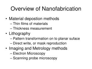
1. 1
2. 2
3. 3
4. 4
5. 5
6. 6
7. 7
8. 8
9. 9
10. 10
11. 11
12. 12
13. 13
14. 14
15. 15
16. 16
17. 17
18. 18
19. 19
20. 20
21. 21
22. 22
23. 23
24. 24
25. 25
26. 26
27. 27
28. 28
29. 29
30. 30
31. 31
32. 32
33. 33
34. 34
35. 35
36. 36
37. 37
38. 38
39. 39
40. 40
41. 41
42. 42
43. 43
44. 44
45. 45
46. 46
47. 47
48. 48 Figure 2 GaAs/GaP nanowire junctions. a, High-resolution TEM of a GaAs/GaP junction grown from a 20-nm gold nanocluster catalyst. Scale bar, 10�nm. Inset, two-dimensional Fourier transforms of the entire image show a splitting of the reciprocal lattice peaks along the 111 , 11 and 00 lattice directions in the [0 2] zone axis, corresponding to the lattice constants for GaAs and GaP (see text). The presence of the heterojunction was confirmed by EDS analysis above and below the junction region (not shown). b, TEM image of another junction. Scale bar, 20�nm. c, d, e, Elemental mapping of the Ga (shown grey), P (red) and As (blue) content of the junction shown in b. A scanning TEM was used to take an elemental 'image' of the junction. f, Line profiles of the composition through the junction region, showing the change in composition as a function of the distance. The slightly higher Ga (shown black) signal relative to the P (red) and As (blue) signals may be due to uncertainties in the detector calibration or the presence of an amorphous gallium oxide layer around the crystalline nanowire core.
Figure 2 GaAs/GaP nanowire junctions. a, High-resolution TEM of a GaAs/GaP junction grown from a 20-nm gold nanocluster catalyst. Scale bar, 10�nm. Inset, two-dimensional Fourier transforms of the entire image show a splitting of the reciprocal lattice peaks along the 111 , 11 and 00 lattice directions in the [0 2] zone axis, corresponding to the lattice constants for GaAs and GaP (see text). The presence of the heterojunction was confirmed by EDS analysis above and below the junction region (not shown). b, TEM image of another junction. Scale bar, 20�nm. c, d, e, Elemental mapping of the Ga (shown grey), P (red) and As (blue) content of the junction shown in b. A scanning TEM was used to take an elemental 'image' of the junction. f, Line profiles of the composition through the junction region, showing the change in composition as a function of the distance. The slightly higher Ga (shown black) signal relative to the P (red) and As (blue) signals may be due to uncertainties in the detector calibration or the presence of an amorphous gallium oxide layer around the crystalline nanowire core.
49. 49 Figure 2 GaAs/GaP nanowire junctions. a, High-resolution TEM of a GaAs/GaP junction grown from a 20-nm gold nanocluster catalyst. Scale bar, 10�nm. Inset, two-dimensional Fourier transforms of the entire image show a splitting of the reciprocal lattice peaks along the 111 , 11 and 00 lattice directions in the [0 2] zone axis, corresponding to the lattice constants for GaAs and GaP (see text). The presence of the heterojunction was confirmed by EDS analysis above and below the junction region (not shown). b, TEM image of another junction. Scale bar, 20�nm. c, d, e, Elemental mapping of the Ga (shown grey), P (red) and As (blue) content of the junction shown in b. A scanning TEM was used to take an elemental 'image' of the junction. f, Line profiles of the composition through the junction region, showing the change in composition as a function of the distance. The slightly higher Ga (shown black) signal relative to the P (red) and As (blue) signals may be due to uncertainties in the detector calibration or the presence of an amorphous gallium oxide layer around the crystalline nanowire core.
Figure 2 GaAs/GaP nanowire junctions. a, High-resolution TEM of a GaAs/GaP junction grown from a 20-nm gold nanocluster catalyst. Scale bar, 10�nm. Inset, two-dimensional Fourier transforms of the entire image show a splitting of the reciprocal lattice peaks along the 111 , 11 and 00 lattice directions in the [0 2] zone axis, corresponding to the lattice constants for GaAs and GaP (see text). The presence of the heterojunction was confirmed by EDS analysis above and below the junction region (not shown). b, TEM image of another junction. Scale bar, 20�nm. c, d, e, Elemental mapping of the Ga (shown grey), P (red) and As (blue) content of the junction shown in b. A scanning TEM was used to take an elemental 'image' of the junction. f, Line profiles of the composition through the junction region, showing the change in composition as a function of the distance. The slightly higher Ga (shown black) signal relative to the P (red) and As (blue) signals may be due to uncertainties in the detector calibration or the presence of an amorphous gallium oxide layer around the crystalline nanowire core.
50. 50
51. 51
52. 52 Nanowire synthesis Nanowires were synthesized either via laser-assisted catalytic growth (GaAs, GaP and InP) or chemical vapour deposition (Si), using Au nanoclusters to direct the growth. Au nanoclusters were deposited onto oxidized silicon substrates and then placed in the reactor furnace. For nanowires produced by laser-assisted catalytic growth, solid targets of GaAs, GaP and InP were ablated using either a pulsed ArF excimer or Nd:YAG lasers, and growth was carried out at 700�850��C in an argon flow of 100�cm3 STP per minute at 100�torr. A pause of 45�s in the ablation was made between each layer in a given superlattice. Silicon nanowires were grown by chemical vapour deposition at 450��C using silane (3�cm3 STP per minute) and either 100�p.p.m. diborane (p) or phosphine (n) in helium (18 �cm3 STP per minute) as dopants. The furnace was evacuated before switching dopants.
The resulting nanowires were sonicated briefly in ethanol and deposited onto copper grids for TEM analysis. The high-resolution TEM images and EDS spectra from nanowire superlattices were collected on a JEOL 2010F microscope. The elemental mapping of the single junction was conducted on a VG HB603 STEM.
Nanowire synthesis Nanowires were synthesized either via laser-assisted catalytic growth (GaAs, GaP and InP) or chemical vapour deposition (Si), using Au nanoclusters to direct the growth. Au nanoclusters were deposited onto oxidized silicon substrates and then placed in the reactor furnace. For nanowires produced by laser-assisted catalytic growth, solid targets of GaAs, GaP and InP were ablated using either a pulsed ArF excimer or Nd:YAG lasers, and growth was carried out at 700�850��C in an argon flow of 100�cm3 STP per minute at 100�torr. A pause of 45�s in the ablation was made between each layer in a given superlattice. Silicon nanowires were grown by chemical vapour deposition at 450��C using silane (3�cm3 STP per minute) and either 100�p.p.m. diborane (p) or phosphine (n) in helium (18 �cm3 STP per minute) as dopants. The furnace was evacuated before switching dopants.
The resulting nanowires were sonicated briefly in ethanol and deposited onto copper grids for TEM analysis. The high-resolution TEM images and EDS spectra from nanowire superlattices were collected on a JEOL 2010F microscope. The elemental mapping of the single junction was conducted on a VG HB603 STEM.
53. 53 Figure 1 Synthesis of core�shell nanowires by chemical vapour deposition. a, Gaseous reactants (red) catalytically decompose on the surface of a gold nanocluster leading to nucleation and directed nanowire growth. b, One-dimensional growth is maintained as reactant decomposition on the gold catalyst is strongly preferred. c, Synthetic conditions are altered to induce homogeneous reactant decomposition on the nanowire surface, leading to a thin, uniform shell (blue). d, Multiple shells are grown by repeated modulation of reactants
Figure 3 Ge�Si core�shell nanowires a, Bright-field image of an unannealed Ge�Si core�shell nanowire with an amorphous p-Si shell. Scale bar is 50�nm. b, c, Scanning TEM elemental maps of Ge (red) and Si (blue) concentrations, respectively, in the nanowire of a. d, High-resolution TEM image of a representative nanowire from the same synthesis as the wire in a�c. Scale bar is 5�nm. e, Elemental mapping cross-section showing the Ge (red circles) and Si (blue circles) concentrations. The solid lines show the theoretical cross-section for a 26-nm-diameter core, 15-nm-thick shell and <1�nm interface according to the model described in the Methods section. f, High-resolution TEM image of annealed Ge�Si core�shell nanowire exhibiting a crystalline p-Si shell. Scale bar is 5�nm. g, Elemental mapping cross-section gives a 5-nm shell thickness with a sharp interface consistent with the TEM image, suggesting that the Ge and Si do not interdiffuse substantially during the annealing process
Figure 1 Synthesis of core�shell nanowires by chemical vapour deposition. a, Gaseous reactants (red) catalytically decompose on the surface of a gold nanocluster leading to nucleation and directed nanowire growth. b, One-dimensional growth is maintained as reactant decomposition on the gold catalyst is strongly preferred. c, Synthetic conditions are altered to induce homogeneous reactant decomposition on the nanowire surface, leading to a thin, uniform shell (blue). d, Multiple shells are grown by repeated modulation of reactants
Figure 3 Ge�Si core�shell nanowires a, Bright-field image of an unannealed Ge�Si core�shell nanowire with an amorphous p-Si shell. Scale bar is 50�nm. b, c, Scanning TEM elemental maps of Ge (red) and Si (blue) concentrations, respectively, in the nanowire of a. d, High-resolution TEM image of a representative nanowire from the same synthesis as the wire in a�c. Scale bar is 5�nm. e, Elemental mapping cross-section showing the Ge (red circles) and Si (blue circles) concentrations. The solid lines show the theoretical cross-section for a 26-nm-diameter core, 15-nm-thick shell and <1�nm interface according to the model described in the Methods section. f, High-resolution TEM image of annealed Ge�Si core�shell nanowire exhibiting a crystalline p-Si shell. Scale bar is 5�nm. g, Elemental mapping cross-section gives a 5-nm shell thickness with a sharp interface consistent with the TEM image, suggesting that the Ge and Si do not interdiffuse substantially during the annealing process
54. 54 Figure 2 GaAs/GaP nanowire junctions. a, High-resolution TEM of a GaAs/GaP junction grown from a 20-nm gold nanocluster catalyst. Scale bar, 10�nm. Inset, two-dimensional Fourier transforms of the entire image show a splitting of the reciprocal lattice peaks along the 111 , 11 and 00 lattice directions in the [0 2] zone axis, corresponding to the lattice constants for GaAs and GaP (see text). The presence of the heterojunction was confirmed by EDS analysis above and below the junction region (not shown). b, TEM image of another junction. Scale bar, 20�nm. c, d, e, Elemental mapping of the Ga (shown grey), P (red) and As (blue) content of the junction shown in b. A scanning TEM was used to take an elemental 'image' of the junction. f, Line profiles of the composition through the junction region, showing the change in composition as a function of the distance. The slightly higher Ga (shown black) signal relative to the P (red) and As (blue) signals may be due to uncertainties in the detector calibration or the presence of an amorphous gallium oxide layer around the crystalline nanowire core.
Figure 2 GaAs/GaP nanowire junctions. a, High-resolution TEM of a GaAs/GaP junction grown from a 20-nm gold nanocluster catalyst. Scale bar, 10�nm. Inset, two-dimensional Fourier transforms of the entire image show a splitting of the reciprocal lattice peaks along the 111 , 11 and 00 lattice directions in the [0 2] zone axis, corresponding to the lattice constants for GaAs and GaP (see text). The presence of the heterojunction was confirmed by EDS analysis above and below the junction region (not shown). b, TEM image of another junction. Scale bar, 20�nm. c, d, e, Elemental mapping of the Ga (shown grey), P (red) and As (blue) content of the junction shown in b. A scanning TEM was used to take an elemental 'image' of the junction. f, Line profiles of the composition through the junction region, showing the change in composition as a function of the distance. The slightly higher Ga (shown black) signal relative to the P (red) and As (blue) signals may be due to uncertainties in the detector calibration or the presence of an amorphous gallium oxide layer around the crystalline nanowire core.