Process Flow
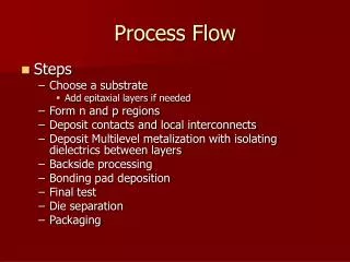
Process Flow. Steps Choose a substrate Add epitaxial layers if needed Form n and p regions Deposit contacts and local interconnects Deposit Multilevel metalization with isolating dielectrics between layers Backside processing Bonding pad deposition Final test Die separation Packaging.

Process Flow
E N D
Presentation Transcript
Process Flow • Steps • Choose a substrate • Add epitaxial layers if needed • Form n and p regions • Deposit contacts and local interconnects • Deposit Multilevel metalization with isolating dielectrics between layers • Backside processing • Bonding pad deposition • Final test • Die separation • Packaging
Introduction • So far, we have studied each of the unit processes of IC fabrication • The details of each process depend on the context in which they are used—i.e., they depend on what comes before and after each step
CMOS Process Flow • A simple CMOS circuit is the inverter • A low on the input prevents the NMOS from conducting and allows the PMOS to conduct, thus drawing the output high • A high on the input allows the NMOS to conduct and prevents the PMOS from conducting, thus pulling the output low
CMOS Process Flow • Must be able to build both NMOS and PMOS together on the same chip • In other circuits, components such as resistors and capacitors may be integrated on the chip
Choosing a Substrate • Type (N or P) • Resistivity (doping level) • Crystal orientation • Wafer size • Wafer flatness • Trace impurities • Most CMOS is built on P-type (100) of moderate resistivity (25-50 -cm) • This corresponds to a doping of about 1015 cm-3
Choosing a Substrate • The typical well doping is 1016 – 1017 cm-3 near the wafer surface • This process is called the “twin well” or “twin tub” process and can be much better controlled by using a higher-doped substrate • The crystal orientation (100) is determined by the low defect concentrations in the SiO2/Si interface in this orientation
Modern CMOS chips have millions of active devices (NMOS and PMOS) side by side in a common silicon substrate • These devices can not interact with each other except via their circuit interconnections • Isolation is obtained by growing a thick layer of SiO2 between each of the active devices • LOCOS (LOCal Oxidation of Silicon).
Wafer After LOCOS • Prior to LOCOS, a thin silicon oxide layer capped with silicon nitride (or a tri-layer of oxide, polysilicon, and nitride) was grown and patterned to prevent a thick oxide from growing everywhere.
Device Isolation: Shallow Trench Isolation • Etch trenches in the Si, which are then fill with a deposited oxide • Process begins as with LOCOS • Fluorine-based etch is used to etch through the nitride, the oxide, and into the wafer • The trenches are approximately 0.5 mm deep
Shallow Trench Isolation • This process eliminates the long time, high temperature LOCOS oxidation • Stresses are not so severe and the film thicknesses do not have to be so tightly controlled • Walls of trenches need to be vertical or slightly sloped; there can be no undercutting • Top and bottom corners of trenches need to be slightly rounded to avoid electrical effects associated with high fields at sharp corners
Shallow Trench Isolation (STI) • A thick layer of SiO2 is deposited by CVD • This process cannot leave gaps or voids in the trenches • Wafer surface is polished using chemical-mechanical polishing (CMP) • to remove the excess oxide and flatten surface
Contact and Local Interconnects • Must be connected electrically together • The first level is called the local interconnect • The first step is to remove the oxide over the source and drain • This etch may be performed without a mask because the oxide to be removed is very thin
Contacts and Local Interconnects • Deposit 50 – 100 nm of Ti over the entire wafer • This is usually done by sputtering • The wafers are then heated in N2 at 600 C for 1 minute • Ti reacts with Si to form TiSi2 where they are in contact • This consumes some Si so the source and drain junctions made deeper than needed.
Contact and Local Interconnects • TiSi2 is an excellent conductor and forms low resistance contacts with the Si and the poly-Si • Ti also reacts with N2 to form TiN (the dotted layer • Also a conductor, but it is not as good as TiSi2. • It is only used for local (short distance) interconnects • Resistance of long lines made of TiN would cause unacceptable RC delays in most circuits
Contact and Local Interconnects • Wafer is then heated to 800 C for 1 min to reduce the resistivity of the TiSi2 to its final value
Multilevel Metal Formation • The final steps are the deposition and patterning of two layers of metal interconnects • At this stage the wafer is highly non-planar. The many layers deposited and patterned leave many hillocks • Problems with discontinuities at the steps and because of thin regions where metal crosses the steps • photolithography is very difficult on non-planar surfaces
Multilevel Metal Formation • Many techniques have been devised to planarize the surface. • A fairly thick layer of SiO2 is deposited on the wafer by CVD or LPCVD. • Layer is thicker than the largest steps on the surface (typically 1 m) • Often doped with either or both P and B to create a phosphosilicate (PSG) or borophosphosilicate glass (BPSG)
Multilevel Metal Formation • Wafer is heated to 800 – 900 C to allow the glass to flow to smooth the surface • Glass reflow does not fully planarize the surface • Layer of photoresist was spun on to fill in the valleys • Wafer is then plasma etched under conditions that etch the photoresist and the SiO2 equally • Etch with no mask until resist (and some of the oxide) is gone
Multilevel Metal Formation Or planarize the surface using CMP
Multilevel Metal Formation • The wafer is now covered with a deposition of TiN or a Ti/TiN bilayer using either sputtering or CVD • Layer is a few tens of nanometers thick • Provides good adhesion to SiO2 and other underlying materials • It also acts as a barrier between the upper metal layers and the lower local interconnect layers • Tungsten (W) is deposited by CVD
Multilevel Metal Formation • The surface is again planarized using CMP to remove the TiN and W everywhere except in the contact holes • This process of etching, filling an planarizing the contact holes is called the damascene process
Multilevel Metal Formation • Metal 1 is deposited (usually) by using sputtering • It is defined using resist and etchback process • Al usually has a small amount of Si and Cu • Cu is now replacing Al in these metal layers • Ti and W layers prevent Cu indiffusion into Si wafer and protect Cu from harsh chemicals used to open dielectrics deposited on top of metalization
Multiple metal levels are deposited by repeating these steps. • After the final metal layer is deposited, a capping protective layer of SiO2 or Si3N4 is deposited • Provides some protection needed for handling during the packaging process • Final anneal at 400-450 C in forming gas • Alloy metal contacts to reduce contact resistance between metal and Si • Reduce the electrical charges in the Si/SiO2 interface
Bonding pads • Thick layer of metalization where connections off-chip are made • Wire bonds • Ball Grid Array (BGA) • Flip-chip metalization (solder) http://www.answers.com/topic/bga http://www.standardics.nxp.com/packaging/lfbga/
http://www.westbond.com/pics/Bond7.jpg http://www.caltexsci.com/CX-3000.htm Wire is compressed into thick metal region on wafer. Ball bond is on the left; wedge bond in on the right. Wedge bonds have a smaller footprint than ball bonds.
Electroplating • Voltage drop between wafer and electrode drives metal ions in a solution to the wafer surface. • Exchange of charge causes ions to become neutral atoms and precipitate out of solution on to wafer. • Thickness of greater than 100 microns can be deposited • Some alloy compositions and low temperature solders can be plated. • Au/Sn, In
Dicing • Diamond edged saw blade. • Wafer mounted on tacky tape, which will be used to transport chips to final test • Wafer surface is protected from chips and debris generated during sawing • Width of saw cut is called a kerf • Usually 2-3 times the width of the saw blade • Damage along kerf can propagate into chip during mechanical, electrical, and thermal stress • Design rules incorporate a margin around area to be cut to minimize the electrical and thermal stress