Understanding Combinational Circuits and Their Role in Digital Logic Design
This guide explores the fundamentals of combinational circuits, highlighting how changes at inputs propagate to outputs without clocking or internal states. It illustrates the differences between combinational logic and memory devices like flip-flops, emphasizes the importance of timing parameters, and addresses common pitfalls such as combinational loops. Additionally, it covers essential components like multiplexers, shifters, and adders, providing insights into their applications in computer architecture and logic design.

Understanding Combinational Circuits and Their Role in Digital Logic Design
E N D
Presentation Transcript
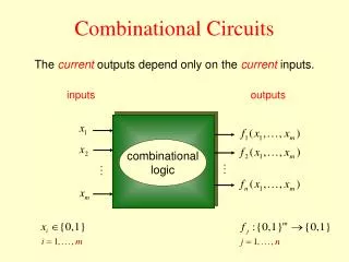
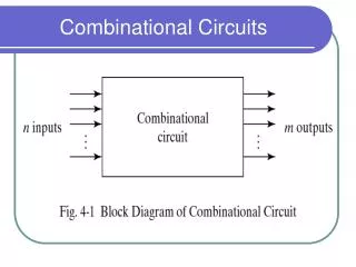
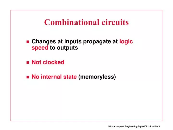
Combinational circuits • Changes at inputs propagate at logic speed to outputs • Not clocked • No internal state (memoryless)
1 Example O I I0 & 1 O I1 & I2
D Q NOT combinational & & S R - latch (has a state) D - flip-flop (clocked, no path)
1 1 1 1 1 1 1 1 Combinational logic - can be connected into sequences - can be connected parallel &
1 1 1 1 1 1 Combinatorial loop This is OK: But what is this?
1 1 1 Combinationial loop 0 1 1 0 Impossible! Logical nonsense Electrical trouble
1 1 1 Combinational loop This is a “combinational loop” We must never have, or form, a combinational loop
D Q How is this usually solved? “The edge-triggered flip-flop!”
D Q The edge-triggered flip-flop! • Never a combinational path from in to out • A memory device, holds the value of “Q” until “clocked” • Ignores the value at “in” until “clocked” in out
D Q Beginners explanation • Flipflop “samples” its input at the rising edge and presents that value on the output. t 1 clock 0 A “rising edge” A “falling edge”
D Q Flip flops in the circuit We will put flip flops in our circuit (Good for “breaking” combinational loops) and clock them all with the same clock
Timing of a positive edge triggered D flip-flop • Setup time, tsetup the time the D input must be stable before the rising edge of the flip-flop. • Hold time, thold the time the D input must be stable after the rising edge of the clock D Clk Q 1, 0 or metastable! t t setup hold If the setup or hold time parameters are violated the Q output will be either logic 0, logic 1 or the flip-flop will enter a metastable state, but will eventually become a valid logic level.
D Clk Q 1, 0 or metastable! t t t hold pLH(CQ) pHL(CQ) t setup Clock to output delay • Clock-to-output delay, tpThe delay of a low to high transition and the delay of a high to low transition may be different.
1 D Q 1 Example BAD OK Suppose the flip flop holds a “1”. Let’s clock this circuit...
D Q 1 Example 0 1 0 Holding Clock “pulse” one “clock cycle”
D Q 1 0 1 0 Example Samples the “0”
D Q 1 0 0 0 Example The exact instant that the output changes!
D Q 1 1 0 1 Example ... the circuit becomes stable again A very short time later... Called a logic “delay” (Propagation through the combinational logic)
D Q 1 1 0 1 Example ... until the next clocking And it stays like that....
Combinational logic in the MIPS • Zero extend box • Sign extend box • Controllable sign/zero extend box • “Tap box” (pick out fields of bits) • Shift left two bits
16 16 16 Zero extend box 16 zeroes ! Out[16..31] In[0..15] Out[0..15]
16 16 16 Sign extend box In[15] copied 16 times Out[16..31] In[0..15] Out[0..15]
16 16 16 Controllable zero / sign extend box Control & Out[16..31] In[15] In[0..15] Out[0..15]
6 5 32 5 5 16 Tap box • Contains no logic circuits • Regroup input bits Opcode field Rs field Instruction Rt field Rd field Immediate field
Shift left two bits Out bit [2..31*] 32 In bit [0..31] Out bit 1 0 Out bit 0 0 * Two bits lost
Arbitrary logic • Given a truth table: A B C D X Y Z 0 0 0 0 1 1 0 0 1 - 1 0 1 - - 1 1 0 1 0 1 • Digital design....... Logic A B C D X Y Z
So, it’s enough just to have the truth table..... We have tools to build the “logic box” “Logic synthesis”
The multiplexor • Special truth table: A B Cont Out 0 - 0 0 1 - 0 1 - 0 1 0 - 1 1 1 • Easy to generalise to “A, B, C, D....” A Out B Cont
"0" msb lsb "0" msb lsb "0" Shifters Two kinds: logical-- value shifted in is always "0" arithmetic-- on right shifts, sign extend Note: these are single bit shifts. A given instruction might request 0 to 32 bits to be shifted!
Example: 4 bit Logical Right Shifter A3 A2 A1 A0 ”0” S0 ”0” S1 If added Right-to-left connections could support Rotate (not in MIPS but found in ISAs)
A3 A2 A1 A0 ”0” S0 = 0 ”0” A3 A1 A2 A0 A3 ”0” A2 S1 = 1 Example: 4 bit logical Right Shifter II • Shift two bits right
Example: 4 bit Right Shifter III A3 A2 A1 A0 ”0” S0 = 0 ”0” A3 A1 A2 A0 A3 ”0” A2 S1 = 1 ”0” ”0” A3 A2 If added Right-to-left connections could support Rotate (not in MIPS but found in ISAs)
S 0 (0,1) S 1 (0, 2) S 2 (0, 4) S 3 (0, 8) General Shift Right Scheme 16 bit using MUXes If added Right-to-left connections could support Rotate (not in MIPS but found in ISAs)
SR3 SR2 SR1 SR0 D3 D2 A2 D1 A1 D0 A0 A3 A2 A1 A0 BarrelShifter (remember?) Technology-dependent solutions: 1 transistor per switch:
32 32 32 What about adders? A[0] A[1] .... A[31] B[0] ....... B[31] C[0] C[1] .... C[31] • Impractical to represent by truth table • Exponential in number of input bits A + C B
Adders are special ..... • We’ll talk about them later • Also, multipliers • Let’s just assume they exist
32 32 32 1 32 32 32 Subtract ? A - B ? = A + NOT (B) + 1 Yes, there’s an easier way... A + 32 B + 1
Controllable Add / Sub ? A B Add Subtract Choose
32 A 32 + 32 32 B =1 Carry in Choose How it’s really done
32 32 32 What’s the point of this ? • The ALU is combinational • Must have control signals to choose! ALU Control points
1 1 1 1 1 32-bit wide inverter ? Out bit[31] In bit[31] Out bit[30] In bit[30] Out bit[1] In bit[1] Out bit[0] In bit[0] 32 32 Easier to draw!
Same idea : • 32 - bit wide multiplexors • 32 - bit wide clocked registers, such as the • Program counter • write back data register 32 32 D Q Clock signal not drawn
Memories ? • Register file • Instruction memory • Data memory • We’ll treat these as combinational (not “clocked”)