Download
1 / 39
390 likes | 554 Vues
Performance estimates for the various types of emerging memory devices. Victor Zhirnov (SRC) and Ramachandran Muralidhar (Freescale). Rationale. We seek to identify fundamental physical limits for various types of memory devices Best projections for scaling

E N D
Performance estimates for the various types of emerging memory devices Victor Zhirnov (SRC) and Ramachandran Muralidhar (Freescale)
Rationale • We seek to identify fundamental physical limits for various types of memory devices • Best projections for scaling • e.g. “no consolidated theory has been developed for Flash scaling Flash Memories, P. Cappelletti et al (Eds), Kluwer 2001
Attributes of an ideal memory • Nonvolatility with long retention (e.g.. > 10 years) • High density • Low power • In-system rewrittability • Fast read/write • High endurance (the number of erase/write/read cycles) • Integration with CMOS logic: • Matching operational voltage • Matching time (speed) Focus of this talk
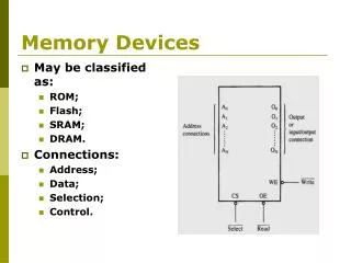
Three Components of Memory Device • Three equally important components of memory systems: • Memory cell (Physics of of Write/Erase/Program) • Sensing (Physics of Read/Sense) • “Wires” (implication of the physics of Write and Read to accessibility) • The key of a cell’s usefulness is whether the cell can be written to and read from without affecting the surrounding cells. Focus of this analysis
ERD ITWG Memory Discussion 10:45 Quantitative estimates of performance for the various types of memories Engineered barrier Muralidhar and Zhirnov Ferroelectric Waser Nanoelectromechanical Zhirnov Fuse/Antifuse Waser and Akinaga 12:00-12:30Lunch Ionic Waser and Akinaga Electronic Effects Waser and Zhirnov Macromolecular Zhirnov Molecular Waser 1:30 Break - Adjourn Memory Discussion
A B e- Control Charge-based Memories DRAM/SRAM Floating Gate Memory SONOS Requirements: 1) Efficient charge injection during programming 2) Suppressed back-flow of charge in store/read modes 3) Efficient erase 4) Min. charge/bit: q=e=1.6x10⁻¹⁹ Q
Store Eb Barrier-less Ohmic Transport: The most efficient injection, but… … difficult retention Write Charge-based memory is a two-barrier system Example: DRAM What is the minimum barrier height for the charge-based NVM?
Eb Thermionic leakage current (ideal case): Min. barrier height for NVM Ebmin What is the minimum barrier height for the charge-based NVM? Store High-barrier are needed for Non-volatile memory Problem: In Si devices Ebmax<Eg=1.1 eV
Charge injection problem in high-barrier systems High-barriers are needed for Non-volatile memory BUT: Barrier formed by an insulating material (large Eb) cannot be suppressed) – charge transport in the presence of barriers: Non-ohmic charge transport Hot-electron injection Tunneling Newly proposed nanomechanical DRAM addresses this problem
Two-barrier charge-based NVM SONOS memory Floating gate memory M. H. White,Y. Yang, A. Purwar, and M. L. French, IEEE Trans. Compon. Packag. and Manufact. Technol.—Pt A 20 (1997) 190 C. Y. Chang, S. M. Sze (Eds.), “ULSI Devices” (John Wiley & sons 2000)
‘0’ FET channel Control gate Floating gate DV DV Floating gate memory: WRITE and STORE modes WRITE STORE leakage
DV We need to create an asymmetry in charge transport through the gate dielectric to maximize the Iwrite/Iret ratio Floating gate cell: Write – triangle barrier Retention – trapezoidal barrier The asymmetry in charge transport between WRITE and STORE modes is achieved through different shape of barrier (triangle vs. trapezoidal)
a Eb DVF-N VW Floating Gate Cell Retention and WRITE characteristics Retention: direct tunneling kBT/e<Vstored<Eb Write: F-N tunneling: DVF-N>Eb The retention time strongly depends on thickness Si/SiO2: Eb=3.1 V, VWSiO2>6.2 V For lower WRITE voltage Eb should be decreased: Ebmin=1.5 eV Vmin>3 V Ideal case
The Industry Standard Flash Memory Cell Flash Memories, P. Cappelletti et al (Eds), Kluwer 2001
This AnalisisSiO2, Eb=3.1eV Vmin>6.8 V (slow operation) V~12 V (ms operation) amin>5.4 nm (reliability issue) Lmin>15 nm (gate stack AR, FET issues…) ‘Optimized’ FG memory cell Eb=1.5 eV HfO2 Vmin>3 V (slow operation) V~4 V (ms operation) amin~6.3 nm Lmin~12 nm Standard FLASHSiO2 Eb=3.1eV - 10-20 V ~6 nm ~18 nm High-K ! Nanocrystals, Charge trapping Parameters Projections for n-FG Flash Memories, P. Cappelletti et al (Eds), Kluwer 2001
Statistical issue Lower bound (slow operation) V~12 V (ms operation) 3x10-16 J Parameters Projections for n-FG SiO2 HfO2 ~2x10-18 F ~6x10-18 F 30 30 1.43x10⁻¹⁷ J 7.2x10⁻¹⁸ J
Materials Challenges of symmetrically graded barrier : fB vs. K Kramers-Kronig relation a=0.2-0.5 K1 <K2 f1<f2
V=0 Eb=2 V Eb=0 V=1 V V=2*Eb=4 V V=2 V Eb=1.5 V Eb=1 V Symmetrically graded (crested) barrier Uses a stack of insulating materials to create a special shape of barrier enabling effective transport into/from the storage node Vw~8 V Likharev, K.K., Single-electron devices and their applications, Proc. IEEE 87 (1999) 606-632
Likharev Engineered tunnel barrier memory
Charge injection problem in high-barrier systems More accurate estimates based on Shockley’s lucky electron model TBD Hot-electron injection
Summary on Floating Gate Memory • Operation voltage cannot be small (e.g. V>6 V for Si/SiO2) • V-t dilemma Question: How to reduce the write voltage for the tunneling based memories? Answer: • To perform write operation in direct tunneling mode • In principle, the voltage can be as small as wished • There are two problems though: • 1) Very slow writing • 2) Very small retention
SONOS For lower voltage operation of floating charge memory, direct tunneling needs to be used for charge injection. Tunnel insulator must be very thin for reasonably small WRITE time We now have a problem of of how to create the asymmetry between WRITE and STORE charge transport paths M. H. White,Y. Yang, A. Purwar, and M. L. French, IEEE Trans. Compon. Packag. and Manufact. Technol.—Pt A 20 (1997) 190
aret d1 d2 d3 SONOS : Write and Retention Retention: Write: Direct tunneling: Vtun<3.1 V, awrite=d1 aret>awrite The asymmetry between WRITE and STORE charge transport paths is achieved by different path length BUT: We now have a problem of of how to create the symmetry between WRITE and ERASE operations X. Wang, et al, IEEE Trans. El. Dev. 51 (2004) 597 Retention??? Erase???
Solutions to improve characteristics of charge-trapping memory? • Alternative dielectrics, e.g. with lower barrier height, high K • Is it possible to control/engineer the trap sites in silicon nitride: concentration, distribution, position, energy levels? X. Wang, et al, IEEE Trans. El. Dev. 51 (2004) 597 HfO2 Ta2O5 HfO2 ERM
Conclusion on ultimate charge-based memories • All charge-based memories suffer from the “barrier” issue: • High barriers needed for long retention do not allow fast charge injection • It is difficult (impossible?) to match their speed and voltages to logic • Voltage-Time Dilemma Non-charge-based NVMs?
Electronic Effects Memory • 1) Charge injection and trapping • Simmons and Verderber, “New conduction and reversible memory phenomena in thin insulating films” • 2) Mott transition • 3) Ferroelectric polarization effects.
Simmons-Verderber theory • Unipolar/non-polar switching • Charging trapes in insulator • ‘Forming process’ is critical • Strongly suggestive of positive ion injection into insulator I 2 ns 100 ns Write Erase
Energy Diagram, V>0 V<f0 (energy of localized levels) V>f0 (energy of localized levels)
Switching (Erase) time estimate Quantum harmonic Oscillator N~1019 cm-3 s~2 nm Etrap~1 eV
Thickness scaling l l N~1019 cm-3 L l~9 nm Lmin~20nm
Scaling limits depend on materials properties N~1019 cm-3 l~9 nm Etrap~1 eV s~2 nm Lmin~20nm tmin~60ns
Macromolecular Memory • Polymer memory • Organic memory • Different mechanisms proposed • Filaments • Ionic • Charged traps in polymer etc • Verbakel et al. “Reproducible resistive switching in nonvolatile organic memories”, APL 91 (2007) • “Resistive switching in organic memories can be due to the presence of a native oxide layer at an aluminum electrode”