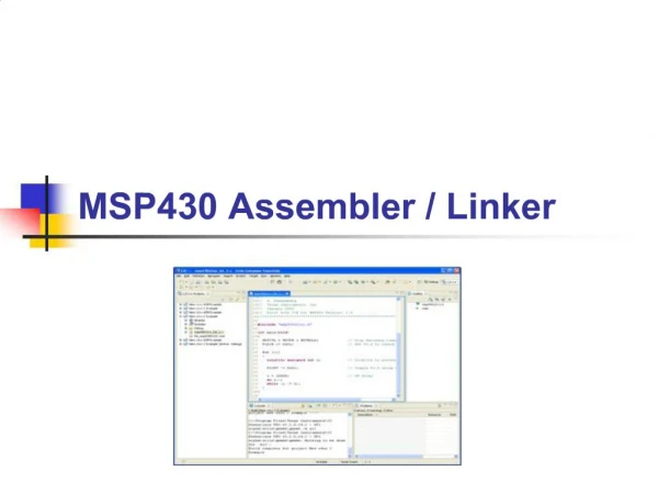
More on MSP430 Programming
More on MSP430 Programming. Administration. Week 17 (6/8): Term Project workshop No class, I will be here to help you work on your term project Deadline for the lab exercises Demo and turn on your codes before 2008/6/8 23:59. Outline. More peripherals Watchdog Timer


More on MSP430 Programming
E N D
Presentation Transcript
Administration • Week 17 (6/8): Term Project workshop • No class, I will be here to help you work on your term project • Deadline for the lab exercises • Demo and turn on your codes before 2008/6/8 23:59
Outline • More peripherals • Watchdog Timer • Supply Voltage Supervisor (SVS) • Direct Memory Access (DMA) • Flash Memory Controller • External 8Mbit Flash Memory: M25P80 • Temperature/humidity sensor: SHT11 • Low Power Modes • MSP430 Software Coding Techniques
Watchdog Timer • Most embedded systems need to be self-reliant • watchdog timer is a hardware • that can watch for system hang • reset the processor if any occur • It is a counter • counts down from some initial value to zero • must select a counter value • periodically restarts the counter • before it counts to zero • If it counts to zero • trigger a system reset
Watchdog timer on MSP430 • 16-bit timer, four software-selectable time intervals • (clock source)/32768, (clock source)/8192, (clock source)/512, (clock source)/64 • Can be configured into watchdog mode or interval mode • Watchdog mode: generate a reset when timer expired • Interval mode: generate a interrupt when timer expired • When power up, it is automatically configured in the watchdog mode • Initial ~32-ms reset interval using the DCOCLK. • Must halt or setup the timer at the beginning
Usage • Stop watchdog timer • WDTCTL = WDTPW + WDTHOLD; • Change watchdog timer interval • WDTCTL = WDTPW+WDTCNTCL+(interval) • Periodically clear an active watchdog • WDTCTL |= WDTPW+WDTCNTCL ClockSource/32768: ClockSource/8192: WDTIS0 ClockSource/512: WDTIS1 ClockSource/64: WDTIS0 + WDTIS1 Password-protected: must include the write password
Example Select clock source: ACLK Select timer interval: (clock source)/8192 = 32768Hz/8192 = 4Hz Reset watchdog counter Reset watchdog counter
Supply Voltage Supervisor • Monitor the AVCC supply voltage or an external voltage • Can be configured to set a flag or generate a reset when the supply voltage or external voltage drops below a user-selected threshold • Comparison • 14 threshold levels for AVCC • External input: SVSIN • compared to an internal level of approximately 1.2 V
SVS Register This bit will set to 1 if the voltage is below threshold • SVSCTL • VLDx
Direct Memory Access • Transfers data from one address to another, without CPU intervention • Increase throughput and decrease power consumption • DMA on MSP430 • Three independent transfer channels • Configurable transfer trigger selections • Timer, UART, SPI, ADC, ….. • Byte or word and mixed byte/word transfer capability • Single, block, or burst-block transfer modes • Block sizes up to 65535 bytes or words
DMA Addressing Modes Source/destination address can be configured to be unchange/increment/decrement after each transfer
DMA Transfer Modes • Six transfer modes • Single transfer, block transfer, burst-block transfer, repeated single transfer, repeated block transfer, repeated burst-block transfer • Single transfer • Each transfer requires a separate trigger, DMA is disable after transfer • Must re-enable DMA before receive another trigger • Repeated single transfer: DMA remains enable • Another trigger start another transfer • Block transfer • Transfer of a complete block after one trigger, DMA is disable after transfer • Repeated block transfer: DMA remains enable, • Another trigger start another transfer • Burst-block transfer • Block transfers with CPU activity interleaved, • Repeated burst-block transfer: DMA remains enable • Keep transferring • CPU executes at 20% capacity
DMA Triggers A transfer is triggered when the CCIFG flag is set A transfer is triggered when USART0 receives new data A transfer is triggered when USART0 is ready to transmit new data A transfer is triggered by an ADC12IFGx flag.
Initialization And Usage • Example (DMACTL0) Configure transfer trigger (DMA0SA) Configure source address (DMA0DA) Configure destination address (DMACTL1) Select transfer mode, addressing mode, and/or other setting, and enable DMA (DMA0SZ) Configure block size Use DMA to transfer a string to UART buffer, send it out through UART Repeated single transfer Source address is incremented source byte to destination byte DMA enable
Others About DMA • DMA Transfer Cycle Time • DMA transfers are not interruptible by system interrupts
Flash Memory Controller • MSP430 flash memory is bit-, byte-, and word-addressable and programmable • Segment erase and mass erase • Minimum VCC voltage during a flash write or erase operation is 2.7 V • Program code are stored in the flash • Unused flash memory can be use to store other data
Flash Memory Characteristics • Write in bit-, byte-, or word; erase in segment • MSP430F1611 segment size • Information memory: 128 bytes • Main memory: 512 bytes • Erase • Make every bit in the segment as logic 1 • Write • Generate logic 0 in the memory • Flash endurance • Maximum erase/write cycles • In MSP430 datasheet • Minimum: 10000 cycles • Typical: 100000 cycles
Flash Memory Operation • Read, write, erase mode • Default mode is read mode • Write/erase modes are selected with the BLKWRT, WRT, MERAS, and ERASE bits • Flash Memory Timing Generator • Sourced from ACLK, SMCLK, or MCLK • Must be in the range from ~ 257 kHz to ~ 476 kHz • Incorrect frequency may result in unpredictable write/erase operation
Flash Memory Erase • Example Disable all interrupts and watchdog (FCTL2) Setup timing generator (FCTL3) Unlock flash memory (FCTL1) Configure the operation Re-enable interrupt and watchdog (FCTL3) lock flash memory Wait until erase complete Dummy write Password protected
Flash Memory Write • Example Disable all interrupts and watchdog (FCTL2) Setup timing generator (FCTL3) Unlock flash memory (FCTL1) Configure the operation Re-enable interrupt and watchdog (FCTL3) lock flash memory Wait until write complete Write to specific memory address Password protected
Outline • More peripherals • Watchdog Timer • Supply Voltage Supervisor (SVS) • Direct Memory Access (DMA) • Flash Memory Controller • External 8Mbit Flash Memory: M25P80 • Temperature/humidity sensor: SHT11 • Low Power Modes • MSP430 Software Coding Techniques
M25P80 • External Flash storage on Taroko • 8 Mbit Flash Memory • SPI Bus Compatible Serial Interface • Memory organization • 16 sectors • Each sector containing 256 pages • Each page is 256 bytes • Operations • Erase: set all bit to 1 • Program(write): reset some bits to 0 • Read: read the content of the flash
SPI • Master–Slave mode • Synchronous protocol • All transmissions are referenced to a common clock • Clock generated by the master (MCU) • Four main signals • Master Out Slave In (MOSI): data from master to slave • Master In Slave Out (MISO): data from slave to master • Serial Clock (SCLK or SCK): clock • Chip Select (CS): select particular peripheral when multiple peripherals are connected to master
Operation • Read Data Bytes (READ) • Read data from memory • Page Program • Write bytes to a page • Up to 256 bytes each time • Sector Erase • sets all bits to 1 inside the chosen sector • Bulk Erase • Erase (sets to 1) all memory data
Device Driver • Download here • http://nslab.ee.ntu.edu.tw/courses/wsn-labs-spring-09/labs/m25p80Driver.rar • Important functions in hal_m25p80.c • void halM25p80Init(void) • void m25p80PowerUp(void); • void m25p80PowerDown(void); • void m25p80PageWrite(UINT16 add, UINT8 *buff, UINT8 size); • void m25p80PageRead(UINT16 add, UINT8 *buff, UINT8 size); • void m25p80SectorErase(UINT8 add); • void m25p80BulkErase(void);
Functions • void m25p80PageWrite(UINT16 add, UINT8 *buff, UINT8 size); • address range from 0x0000 to 0x0fff (4096 pages in total) • At most 256 bytes • Always write from the beginning of the page • void m25p80PageRead(UINT16 add, UINT8 *buff, UINT8 size); • address range from 0x0000 to 0x0fff (4096 pages in total) • At most 256 bytes • Always read from the beginning of the page • void m25p80SectorErase(UINT8 add); • address range from 0x00 to 0x0f (16 sectors in total) • Each sector is 65536 bytes
Outline • More peripherals • Watchdog Timer • Supply Voltage Supervisor (SVS) • Direct Memory Access (DMA) • Flash Memory Controller • External 8Mbit Flash Memory: M25P80 • Temperature/humidity sensor: SHT11 • Low Power Modes • MSP430 Software Coding Techniques
SHT11 • Relative humidity and temperature sensors • Digital output • Manufacturer defined interface • two wires bi-direction Use a GPIO pin as clock (SCK), it is always output direction Use another GPIO as DATA, dynamic setting it to input(read) or output(write) direction
Start Transmission and Send Command • How to start • What are the commands available
An Example: SHT11 Pull-up Data pin in output direction Set data pin to input direction, then SHT11 controls the DATA line • Timing diagram
Convert to Physical Values • 12-bit humidity, 14-bit temperature • Temperature • Humidity
Device Driver • Download here • http://nslab.ee.ntu.edu.tw/courses/wsn-labs-spring-09/labs/sht11Driver.rar • Important functions in SHT1x_sensirion.c • void sht1xInit(); • void sht1xReset(); • char sht1xMeasure(unsigned char *p_value, unsigned char *p_checksum, unsigned char mode); • void sht1xCalculate(float *p_humidity ,float *p_temperature);
Functions • char sht1xMeasure(unsigned char *p_value, unsigned char *p_checksum, unsigned char mode); • mode: { TEMP, HUMI } • Store measured value to *p_value • Store 8-CRC checksum to *p_checksum • void sht1xCalculate(float *p_humidity ,float *p_temperature); • Convert measured value to physical value • Put the measured value in *p_humidity, *p_temperature • Result will also place in *p_humidity, *p_temperature (overwrite)
Outline • More peripherals • Watchdog Timer • Supply Voltage Supervisor (SVS) • Direct Memory Access (DMA) • Flash Memory Controller • External 8Mbit Flash Memory: M25P80 • Temperature/humidity sensor: SHT11 • Low Power Modes • MSP430 Software Coding Techniques
MSP430 Clock System high-frequency oscillator (optional) MSP430 digitally controlled oscillator Clock Signals Clock Modules CPU DCOCLK MCLK: Master Clock XT2CLK SMCLK: Sub-main clock Peripherals: Timer, UART, … LFXT1CLK ACLK: Auxiliary clock 32.768KHz fixed rate Low-frequency/high-frequency oscillator
MSP430 Power Consumption Characteristics • Current increase with clock frequency • Current increase with supply voltage • Supply voltage vs frequency • More active peripherals means more current consumption
Operating Modes • MSP430 has six operating modes • The operating modes take into account three different needs • Ultralow-power • Speed and data throughput • Minimization of individual peripheral current consumption • Turn off different clocks in different operating mode
Low Power Modes • Different low power mode disable different clocks • Peripherals operating with any disabled clock are disabled until the clock becomes active • Wake up is possible through all enabled interrupts • Returns to the previous operating mode if the status register value is not altered during the ISR