CMOS image sensors
CMOS image sensors. Presenter: Alireza eyvazzadeh. Complementary metal–oxide–semiconductor. a technology for constructing integrated circuits. CMOS technology is used in Microprocessors Microcontrollers static RAM other digital logic circuits.


CMOS image sensors
E N D
Presentation Transcript
CMOS image sensors Presenter: Alirezaeyvazzadeh
Complementary metal–oxide–semiconductor a technology for constructing integrated circuits CMOS technology is used in Microprocessors Microcontrollers static RAM other digital logic circuits CMOS technology is also used for several analog circuits such as image sensors data converters
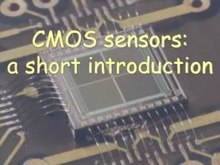
CMOS image sensors Two most common types of sensors used in digital cameras: CCD - Charge Coupled Device CMOS - Complementary Metal Oxide Semiconductor All CCD and CMOS image sensors operate by exploiting the photoelectric effect to convert light into electricity With the CMOS imager both the 'Photon-to-Electron' conversion and the 'Electron-to-Voltage' conversion is done within the pixel
Some drawbacks of CCDs complex clocking requirements high power consumption difficulty of on-chip integration of circuitry limited frame rate CMOS image sensors address these drawbacks by using the same technology as microprocessors and memory chips
Advantages and drawbacks of the CMOS image sensors Low Power Consumption one-third to more than 100 times less than that of CCDs Lower cost compared to CCD’s technology On chip functionality A sensor can integrate various signal and image processing blocks such as amplifiers, ADCs, circuits for color processing and data compression, etc. on the same chip Miniaturization High-speed imaging Random access of image data Selective read-out mechanism Also they are still too noisy and less sensitive than CCDs
present applications of CMOS image sensors internet camera digital still camera machine vision Automotive children’s toy medicine and dentistry fingerprint ID surveillance aerospace motion analysis industrial inspection quality control process control target tracking spectroscopy
Overall architecture CMOS imagers architecture can be divided into four main blocks: 1. Pixel Array 2. Analog Signal Processors 3. Row and Column Selector 4. Timing and Control
Basic pixel structures Each pixel contains a photodetector and some transistors. This area is the heart of an image sensor and the imaging quality is largely determined by the performance of this area. active pixels (APS) passive pixels (PPS) Pixel circuits An APS has three transistors in a pixel, while a PPS has only one transistor. To achieve further improvement, an advanced APS that has four transistors in a pixel, the so-called 4T-APS, has been developed. APS are sensors that implement a buffer per pixel. Currently, APS are the predominant devices, although in some cases PPS are also used. The in-pixel amplifier in APS enables non-destructive read of the photodiode charge at a faster speed and a generally higher signal-to-noise ratio (SNR) than PPS
Operation of a photodetector comprises: • generation of free electron-hole pairs due to impinging light • separation and collection of electrons and holes • (c) production of an output signal through interaction with other components Several popular silicon-based photosensing devices are Photoconductors PN and PIN photodiodes Phototransistors photogates
PN junction photodiode an important sensor for digital imaging The potential voltage decreases when electrons accumulate. By measuring the voltage drop, the total amount of light power can be obtained.
Active pixel sensor, 3T-APS First, the reset transistor MRS is turned on PD is reset to the value Vdd −Vth Vth is the threshold voltage of transistor MRS MRS is turned off and the PD is electrically floated The accumulated charge changes the potential in the PD; the voltage of the PD,VPD ,decreases according to the input light intensity After an accumulation time, the select transistor MSEL is turned on and the output signal in the pixel is read out in the vertical output line. When the read-out process is finished MSEL is turned off and MRS is again turned on to repeat the above process.
Sensor peripherals Addressing In CMOS image sensors, to address each pixel, a scanner or a decoder is used Readout circuits The voltage of a PD is read with a source follower (SF) a follower transistor MSF is placed in a pixel and a current load Mb is placed in each column