
Innovations in Lithography Double Patterning Techniques for Enhanced Resolution Limit
E N D
Presentation Transcript
Double Patterning Samuel Johnson 11/6/18
Outline • Background • Introduction to SADP • Deposition • Trim mask issue • Self Aligned Quadruple Patterning • SADP Problems • Via Level Manufacturing
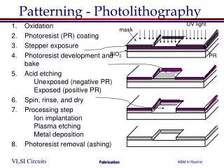
Single Patterning • Lithography and Etch • Lay photoresist • Lithography • Develop Chris Mack Lecture 59 (CHE 323) Lithography Double Manufacturing
Single Patterning Resolution Limit • Theoretical Limit at 36nm • Formula is for half pitch: full pitch is 80nm https://http://www.aspdac.com/aspdac2013/archive/pdf/3C-4.pdf/
Two Lithography Double Patterning • Litho-etch-Litho-Etch • Litho-freeze-Litho-Etch Chris Mack Lecture 59 (CHE 323) Lithography Double Manufacturing
Two Lithography Double Patterning • Problems • Expensive: two lithography steps • Overlay problem https://semiengineering.com/fillcut-self-aligned-double-patterning/
Self Aligned Double Patterning Nakatama, K; et al. SPIE 2012
Conformal Deposition • Step 3: Deposition of sidewall material • Thickness of deposited layer is crucial Chris Mack Lecture 59 (CHE 323) Lithography Double Manufacturing
Chemical Vapor Deposition (CVD) • Deposition method of choice • Able to deposit on resist material and wafer • High quality • Anisotropic process • Industrially viable Chris Mack Lecture 59 (CHE 323) Lithography Double Manufacturing
Chemical Vapor Deposition (CVD) • CVD is simple and cheap • High temperature • Meets criteria listed before
Etching • Etch time and conditions will determine material etched • Etching too long will result in different sized features https://semiengineering.com/fillcut-self-aligned-double-patterning/
Trim Mask Issue • Sidewall forms all around patterns-loops • A problem if not desired Chris Mack Lecture 59 (CHE 323) Lithography Double Manufacturing
Trim Masks • Use another lithography step to get rid of undesired material • Second mask • Only use to get rid of unnecessary patterns https://ieeexplore.ieee.org/document/7723830
Trim Masks • Overlay becomes a problem • Alignment of the second mask becomes a consideration https://ieeexplore.ieee.org/document/7723830
Trim Masks • Second SADP Lithography step is simpler than a second LELE Lithography step • Cheaper • Less Critical https://semiengineering.com/self-aligned-double-patterning-part-one/
Self Aligned Quadruple Patterning • “Double SADP” • Doubles resolution • Two trim lithography steps Nakatama, K; et al. SPIE 2012
Self Aligned Quadruple Patterning Nakatama, K; et al. SPIE 2012
SADP Problems • Not all patterns can be printed • Primary and secondary patterns can’t touch https://http://www.aspdac.com/aspdac2013/archive/pdf/3C-4.pdf/
SADP Problems • Anti-parallel line ends • Trim masks overlap if they are too close https://ieeexplore.ieee.org/document/7723830
SADP Problems • Turns are difficult to control • Unideal patterning results https://ieeexplore.ieee.org/document/7723830
SADP Problems-Via Manufacturing • Via manufacturing with SADP or single patterning is not possible • Requires another double lithography technique https://ieeexplore-ieee-org.ezproxy.lib.utexas.edu/document/7940014
Via Manufacturing • Double manufacturing with half absorbance • The common exposed areas are fully exposed
Via Manufacturing • After etching, unexposed areas form holes • Holes can be filled with a conductive via material
Via Manufacturing • Via connects different layers of materials • Other layers formed from other types of patterning
Conclusions • SADP along with other multiple patterning techniques will continue to be useful • Combination of multiple patterning techniques • Design considerations will dominate what manufacturing method is used • Future innovations in multiple patterning are required to continue Moore’s Law until NGL’s are feasible
References • Self-Aligned Double Patterning Lithography Aware Detailed Routing With Color Preassignment - IEEE Journals & Magazine, ieeexplore.ieee.org/document/7723830. • Self-Aligned Double Patterning-Aware Detailed Routing with Double via Insertion and via Manufacturability Consideration - IEEE Conference Publication, ieeexplore.ieee.org/document/7544285. • “Fill/Cut Self-Aligned Double-Patterning.” Semiconductor Engineering, semiengineering.com/fillcut-self-aligned-double-patterning/. • Mack, Chris. “Lecture 59 (CHE 323) Lithography Double Patterning.” YouTube, YouTube, 8 Nov. 2013, www.youtube.com/watch?v=Foush3X7dCc. • Nakayama, Koichi, et al. “Self-Aligned Double and Quadruple Patterning Layout Principle.” Search the World's Largest Collection of Optics and Photonics Applied Research., International Society for Optics and Photonics, 14 Mar. 2012, www.spiedigitallibrary.org/conference-proceedings-of-spie/8327/83270V/Self-aligned-double-and-quadruple-patterning-layout-principle/10.1117/12.916678.full. • “Self-Aligned Double Patterning, Part One.” Semiconductor Engineering, semiengineering.com/self-aligned-double-patterning-part-one/. • “Triple Patterning and Self-Aligned Double Patterning (SADP).” Tech Design Forum Techniques, www.techdesignforums.com/practice/guides/triple-patterning-self-aligned-double-patterning-sadp/.