Download
1 / 14
140 likes | 337 Vues
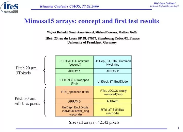
Mimosa15 arrays: concept and first test results. Wojtek Dulinski, Samir Amar-Youcef, Michael Deveaux, Mathieu Goffe IReS, 23 rue du Loess BP 28, 67037, Strasbourg Cedex 02, France University of Frankfurt, Germany. 3T RTol, S-D optimum (second)). UniDepl, 3T, RTol, Common Nwell ring.

E N D
Mimosa15 arrays: concept and first test results Wojtek Dulinski, Samir Amar-Youcef, Michael Deveaux, Mathieu Goffe IReS, 23 rue du Loess BP 28, 67037, Strasbourg Cedex 02, France University of Frankfurt, Germany 3T RTol, S-D optimum (second)) UniDepl, 3T, RTol, Common Nwell ring Pitch 20 µm, 3Tpixels ARRAY 1 ARRAY 2 3T RTol, S-D swapped (first) UniDepl, 3T, EnclDiode RTol, LOCOS totally removed(first) RTol_optimized (first) Pitch 30 µm, self-bias pixels ARRAY3 ARRAY 0 UniDepl, Encl.Diode, individual Nwell_ring (second)) RTol, 3T Self Bias (second)) Size (all arrays): 42x42 pixels
55Fe calibration tests: Temperature: -25°C, 10°C and 40°C Integration time: 200 µs (10MHz) and 800 µs (2.5 MHz) To be compared with Mimosa 11 results -25 °C 10°C 40 °C 0 krad Standard diode Rad-tol diode
Mimosa15: Array0, Sub1 (C1S1)Optimization of M*2 RadTol type diode Diode dimension: 3.6x4.4 µm2 ENC = 11.1÷ 19.2 el (« Standard » RadTol (3.4x4.3 µm2): ENC = 12÷ 16 el )
Mimosa15: Array3, Sub2 (C4S1)LOCOS totally removed Diode dimension: 3.6x4.4 µm2 ENC = 14.8÷ 26 el
Mimosa15: Array3, Sub1 (C4S2)3T self-bias Diode dimension: 3.6x4.4 µm2 ENC = 14.1÷ 22.1 el
Conclusions 1Do we have arguments to adjust the diode design on Mimo*3?Not obvious, check after irradiation! Not STRONG arguments, if any…
Mimosa15: Array1, Sub1 (C2S1)3T-RadTol, “swapped” (less optimum for noise) S-D on Reset Transistor Diode dimension: 4x4 µm2 ENC = 16.1÷ 20.1 el
Mimosa15: Array1, Sub2 (C2S2)3T-RadTol, “standard” (optimum for noise) S-D on Reset Transistor Diode dimension: 4x4 µm2 ENC = 11.6÷ 15.2 el
Conclusions 2Charge losses on “standard” after irradiation???
Mimosa15: Array0, Sub2 (C1S2)UniDepleted Self-bias, Enclosed Diode, Individual Nwell ring, All- Periphery Pwell Ring Diode dimension: 8x5.2 µm2 ENC = 15.3÷ 17.8 el
Mimosa15: Array2, Sub1 (C3S1)3T Non RadTol, Enclosed Diode, NO Nwell ring Diode dimension: 5.2x5.2 µm2 ENC = 12.4÷ 19.7 el
Mimosa15: Array2, Sub2 (C3S2)3T RadTol, Common Nwell ring, Small Corner Pwell for substrate current injection Diode dimension: 4x4 µm2 ENC = 12.3÷ 19.5 el
Conclusions 3A0S2: No significant changes in spectrum for I+=I-=3µA (like in Mimosa11).But where I+ current goes? Very low contact resistivity!A2S1 and A2S2: Impossible to inject the current! Diode instead of ohmic contact??? Too small dimension of Pwell or “smoothing” during mask generation?
Which structure for EM imaging?No clear answer, unfortunately… Shall we try the new idea?