Microcontact Printing (Soft Lithography)
Microcontact Printing (Soft Lithography). Outline. Motivation History Schematic Procedure Photomask Snowflake "I Love NanoLab" OU interlock logo Stamp Master The stamp Chemistry of the Process Transferring the Pattern Etching the Substrate Examples. Motivation.

Microcontact Printing (Soft Lithography)
E N D
Presentation Transcript
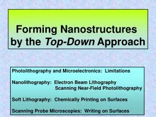
Outline • Motivation • History • Schematic • Procedure • Photomask • Snowflake • "I Love NanoLab" • OU interlock logo • Stamp Master • The stamp • Chemistry of the Process • Transferring the Pattern • Etching the Substrate • Examples
Motivation • Production of silicon integrated circuits • Patterning biological macromolecules, organic and inorganic salts, colloidal materials, conducting polymers, polymer beads • The figure to the right is a patterned rod Image courtesy of Jackman et al, Science 1998. vol. 280(5372) pp 2089-2091
Motivation: Novel Example • Transferring micrometer size pattern onto various surfaces • Surface does not have to be flat (as opposed to photolithography) • The figure to the right is an example of how one would transfer patterns to a cylindrical rod Image courtesy of Jackman et al, Science 1998. vol. 280(5372) pp 2089-2091
History • Both lithography and stamp printing have been around for centuries • It was the combination of the two that gave rise to microcontact printing • In 1993, Amit Kumar and George M. Whitesides developed microcontact printing at Harvard University • Subsequent methods of soft lithography have since been explored • In 1996 IBM began research on improving optical lithography in order to enhance the precision of the printing process
Process Schematic A prepolymer (2) covering the master (1) is cured by heat or light and demolded to form an elastomeric stamp (3), which is inked by immersion (4) or with an ink pad (5) and printed onto the substrate (6), forming a self-assembled monolayer, which is transferred into the substrate by a selective etch. Scanning electron micrographs show the master, image of the stamp, and the printed and etched pattern. Image taken from http://www.aip.org/tip/INPHFA/vol-8/iss-4/p16.pdf
Photomask opaque • Create desired pattern on computer (AutoCAD, Adobe Illustrator, or your favorite graphics program) • Print onto transparency • Further reduction of size can done photographically • Pattern must be in solid black and white and printed using an opaque ink, which is determined by the photoresist
About the Photomask: Snowflake • The snowflakes in the photomask are made such that each subsequent one was half the size of the previous one • Measurements were made regarding snowflake size as well as distance between the snowflakes • These measurements were used to evaluate how well the pattern transfer occurred • The depth of the stamp was determined (determined by the master): • If the stamp is too shallow, there can be contact in between the features • If the stamp is too deep, the features can be distorted 0.629 mm 11.3 mm 9.175 mm From Whitesides et. al paper
About the Photomask: "I Love Nanolab" • In this photomask, “I Love Nanolab” the largest text (#1) are 3mm by 21.3 mm. Each subsequent set is half the size of the previous. • The smallest size (#8) is 128 times smaller than the biggest size, and is 23.4µm X 166.4µm 21.3 mm 3 mm Don’t YOU love NanoLab?
About the Photomask: OU Logo • In this photomask, the largest OU logo is 10 mm wide and 13.7 mm long. 10 mm 13.7 mm
Stamp Master (mold) • Done on glass slide using the mask as the source of the pattern • Apply photoresist (10-20 μm) • (MicroChem SU-8 2010) Spin coat for even distribution • Cover Sample with Mask and Expose to UV light • The resist will harden upon exposure (negative resist) • Soft-Baking • Put on hotplate, or oven for 3 minutes • Develop • Unexposed resist will be dissolved, while the exposed resist remains • Wash Master and clean up
The Stamp • Clean master sample and place in walled container (disposable petri dish). • Pour silicone resin evenly over master • The silicone resin is liquid polydimethylsiloxane [PDMS] • Bake the PDMS to solidify (65C for 15-20h). • Remove cured stamp from master and wash both in EtOH
Chemistry of the Process • Stamp is inked with a thiol (R-S-H) • The thiol ink pattern is stamped onto the metal surface • The thiol ink works as an etch resist • Etching removes metal on uninked areas • A thiol ink is ~2mM solution of hexadecanethiol • The substrate is a Pd or Au thin film evaporated on polished Si wafer
Transferring the Pattern to a Thin Metal Film • Wash both substrate (the metal) and the stamp in EtOH • Using Q-Tip, coat the stamp with the thiol solution and dry it • dry under N2 stream for ~30sec • Bring stamp into contact with substrate for 10 sec., remove stamp and dry substrate under N2
Useful Chemistry • The sulfur atoms bonds to the metal (Pd or Au) • The carbon chains of the thiol will then align with each other to create a hydrophobic SAM (self-assembling monolayer) • The monolayer acts as a protective coating against the etchant • The best results are often obtained by the longest chains because they create a larger and therefore better barrier
Etching the Substrate • Immerse substrate in diluted (1:3) etchant for <30 sec (Pd Etchant, type TFP inCYANIDE!!!– be careful, it’s highly toxic!) • The time here is very important!!! If you leave it too long in the etch, you will most likely remove ALL the Pd, if it’s not long enough, then your pattern will not be fully developed. • Remove from etchant and immediately quench it in deionized water, rinse and dry.
Good and Bad Examples: Black lines drawn to mark the edge of the snowflakes