Download
1 / 100
1k likes | 1.19k Vues
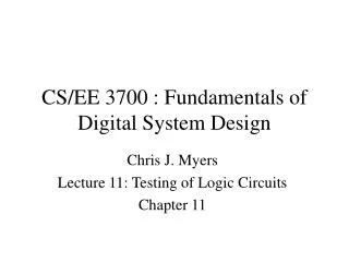
CS/EE 3700 : Fundamentals of Digital System Design. Chris J. Myers Lecture 7: Flip-flops, Registers, Counters Chapter 7. Sequential Circuits. Combinational – output depends only on the input. Sequential – output depends on input and past behavior. Require use of storage elements.

E N D
CS/EE 3700 : Fundamentals of Digital System Design Chris J. Myers Lecture 7: Flip-flops, Registers, Counters Chapter 7
Sequential Circuits • Combinational – output depends only on the input. • Sequential – output depends on input and past behavior. • Require use of storage elements. • Contents of storage elements is called state. • Circuit goes through sequence of states as a result of changes in inputs.
Set Sensor ¤ On Off Memory Alarm element Reset Figure 7.1 Control of an alarm system
A B Figure 7.2 A simple memory element
Load A B Output Data TG1 TG2 Figure 7.3 A controlled memory element
Reset Set Q Figure 7.4 A memory element with NOR gates
Q S R Q R a b Q a (no change) 0 0 0/11/0 0 1 0 1 1 0 1 0 1 1 0 0 Q b S (a) Circuit (b) Truth table t t t t t t t t t t 1 2 3 4 5 6 7 8 9 10 1 R 0 1 S 0 1 Q ? a 0 1 Q ? b 0 Time (c) Timing diagram Figure 7.5 A latch built with NOR gates
( ) Q t + 1 Clk S R ¢ R R Q 0 x x Q( t ) (no change) 1 0 0 Q( t ) (no change) Clk 1 0 1 0 1 1 0 1 Q 1 1 1 x S ¢ S (a) Circuit (b) Truth table 1 Clk 0 1 R 0 Q S 1 Clk S 0 R Q 1 ? Q 0 (d) Graphical symbol 1 ? Q 0 Time (c) Timing diagram Figure 7.6 Gated SR latch
S Q Clk Q R Figure 7.7 Gated SR latch with NAND gates
S D (Data) Q Clk Q R (a) Circuit ( ) Clk D Q t + 1 Q D ( ) Q t 0 x 1 0 0 Clk Q 1 1 1 (b) Truth table (c) Graphical symbol Figure 7.8 Gated D latch
S D (Data) Q Clk Q R (a) Circuit t t t t 1 2 3 4 Clk D Q Time (d) Timing diagram Figure 7.8 Gated D latch
t su t h Clk D Q Figure 7.9 Setup and hold times
Master Slave Q Q m s Q Q D D Q D Clk Clk Clock Q Q Q (a) Circuit Clock D Q D Q m Q Q = Q s (b) Timing diagram (c) Graphical symbol Figure 7.10 Master-slave D flip-flop
Q D Clock Q (b) Graphical symbol 1 P3 P1 2 5 Q Clock 6 Q P2 3 4 P4 D (a) Circuit Figure 7.11 A positive-edge-triggered D flip-flop
Clock D Q a Q b Q c (b) Timing diagram Q D D Q a Clock Q Q Clk a Q D Q b Q Q b Q Q D c Q Q c (a) Circuit Figure 7.12 Comparison of level-sensitive and edge-triggered
Preset D Q Clock Q Clear (a) Circuit Preset Q D Q Clear (b) Graphical symbol Figure 7.13 Master-slave D flip-flop with Clear and Preset
Preset Q Clock Q Preset Q D D Q Clear Clear (a) Circuit (b) Graphical symbol Figure 7.14 Positive-edge-triggered D flip-flop with Clear and Preset
( ) Q t + 1 T ( ) 0 Q t ( ) 1 Q t Q D Q (b) Truth table T Q Q Q T Clock Q (a) Circuit (c) Graphical symbol Clock T Q (d) Timing diagram Figure 7.16 T flip-flop
J Q D Q K Q Q Clock (a) Circuit Q ( t + 1 ) J K 0 0 Q ( t ) J Q 0 1 0 1 0 1 K Q 1 1 Q ( t ) (b) Truth table (c) Graphical symbol Figure 7.17 JK flip-flop
Summary of Terminology • Basic latch – cross-coupled NAND/NOR • Gated latch – output changes when clk = 1. • Gated SR latch • Gated D latch • Flip-flop – output changes only on clk edge. • Edge-triggered flip-flop • Master-slave flip-flop
Q Q Q Q 1 2 3 4 In Out Q Q Q Q D D D D Clock Q Q Q Q (a) Circuit Q Q Q Q = Out In 1 2 3 4 t 1 0 0 0 0 0 t 0 1 0 0 0 1 t 1 0 1 0 0 2 t 1 1 0 1 0 3 t 1 1 1 0 1 4 t 0 1 1 1 0 5 t 0 0 1 1 1 6 t 0 0 0 1 1 7 (b) A sample sequence Figure 7.18 A simple shift register
Parallel output Q Q Q Q 3 2 1 0 Q Q Q Q D D D D Q Q Q Q Serial Clock Shift/Load input Parallel input Figure 7.19 A simple shift register
1 Q Q Q T T T Clock Q Q Q Q Q Q 0 1 2 (a) Circuit Clock Q 0 Q 1 Q 2 Count 0 1 2 3 4 5 6 7 0 (b) Timing diagram Figure 7.20 A three-bit up-counter
1 Q Q Q T T T Clock Q Q Q Q Q Q 0 1 2 (a) Circuit Clock Q 0 Q 1 Q 2 Count 0 7 6 5 4 3 2 1 0 (b) Timing diagram Figure 7.21 A three-bit down-counter
Clock cycle Q Q Q 2 1 0 Q changes 1 0 0 0 0 Q changes 2 1 0 0 1 2 0 1 0 3 0 1 1 4 0 0 1 5 1 0 1 6 1 0 1 7 1 1 1 8 0 0 0 Table 7.1 Derivation of the synchronous up-counter
1 Q Q Q Q T T T T Q Q Q Q 0 1 2 3 Clock Q Q Q Q (a) Circuit Clock Q 0 Q 1 Q 2 Q 3 Count 0 1 2 3 4 5 6 7 8 9 10 11 12 13 14 15 0 1 (b) Timing diagram Figure 7.22 A four-bit synchronous up-counter
Enable Q Q Q Q T T T T Clock Q Q Q Q Clear Figure 7.23 Inclusion of enable and clear capability
Q Q D 0 Enable Q Q Q D 1 Q Q Q D 2 Q Q Q D 3 Q Output carry Clock Figure 7.24 A four-bit counter with D flip-flops
0 Enable Q Q D 0 1 D 0 Q 0 Q Q D 1 D 1 1 Q 0 Q Q D 2 D 1 2 Q 0 Q Q D 3 D 1 3 Q Output carry Load Clock Figure 7.25 A counter with parallel-load capability
Enable 1 D Q 0 0 0 D Q 0 1 1 D Q 0 2 2 Load Clock Clock (a) Circuit Clock Q 0 Q 1 Q 2 Count 0 1 2 3 4 5 0 1 (b) Timing diagram Figure 7.26 A modulo-6 counter with synchronous reset
1 Q Q Q T T T Q Q Q 0 1 2 Clock Q Q Q (a) Circuit Clock Q 0 Q 1 Q 2 Count 0 1 2 3 4 5 0 1 2 (b) Timing diagram Figure 7.27 A modulo-6 counter with asynchronous reset
Enable 1 D Q 0 0 0 D Q 0 1 1 BCD D Q 0 0 2 2 Q D 0 3 3 Load Clock Clock Enable Clear D Q 0 0 0 D Q 0 1 1 BCD 1 D Q 0 2 2 D Q 0 3 3 Load Clock Figure 7.28 A two-digit BCD counter
Q Q Q 0 1 n – 1 Q Q Q D D D Q Q Q Reset Clock Figure 7.30 Johnson counter
Data Clock Latch Figure 7.32 Gated D latch generated by CAD tools
LIBRARY ieee ; USE ieee.std_logic_1164.all ; LIBRARY altera ; USE altera.maxplus2.all ; ENTITY flipflop IS PORT ( D, Clock : IN STD_LOGIC ; Resetn, Presetn : IN STD_LOGIC ; Q : OUT STD_LOGIC ) ; END flipflop ; ARCHITECTURE Structure OF flipflop IS BEGIN dff_instance: dff PORT MAP ( D, Clock, Resetn, Presetn, Q ) ; END Structure ; Figure 7.35 Instantiating a D flip-flop from a package
LIBRARY ieee ; USE ieee.std_logic_1164.all ; ENTITY implied IS PORT ( A, B : IN STD_LOGIC ; AeqB : OUT STD_LOGIC ) ; END implied ; ARCHITECTURE Behavior OF implied IS BEGIN PROCESS ( A, B ) BEGIN IF A = B THEN AeqB <= '1' ; END IF ; END PROCESS ; END Behavior ; Figure 7.36 Implied memory
LIBRARY ieee ; USE ieee.std_logic_1164.all ; ENTITY latch IS PORT ( D, Clk : IN STD_LOGIC ; Q : OUT STD_LOGIC) ; END latch ; ARCHITECTURE Behavior OF latch IS BEGIN PROCESS ( D, Clk ) BEGIN IF Clk = '1' THEN Q <= D ; END IF ; END PROCESS ; END Behavior ; Figure 7.37 Code for a gated D latch
LIBRARY ieee ; USE ieee.std_logic_1164.all ; ENTITY flipflop IS PORT ( D, Clock : IN STD_LOGIC ; Q : OUT STD_LOGIC) ; END flipflop ; ARCHITECTURE Behavior OF flipflop IS BEGIN PROCESS ( Clock ) BEGIN IF Clock'EVENT AND Clock = '1' THEN Q <= D ; END IF ; END PROCESS ; END Behavior ; Figure 7.38 Code for a D flip-flop
LIBRARY ieee; USE ieee.std_logic_1164.all; ENTITY flipflop IS PORT ( D, Clock : IN STD_LOGIC ; Q : OUT STD_LOGIC ) ; END flipflop ; ARCHITECTURE Behavior OF flipflop IS BEGIN PROCESS BEGIN WAIT UNTIL Clock'EVENT AND Clock = '1' ; Q <= D ; END PROCESS ; END Behavior ; Figure 7.39 Code for a D flip-flop using WAIT UNTIL
LIBRARY ieee ; USE ieee.std_logic_1164.all ; ENTITY flipflop IS PORT ( D, Resetn, Clock : IN STD_LOGIC ; Q : OUT STD_LOGIC) ; END flipflop ; ARCHITECTURE Behavior OF flipflop IS BEGIN PROCESS ( Resetn, Clock ) BEGIN IF Resetn = '0' THEN Q <= '0' ; ELSIF Clock'EVENT AND Clock = '1' THEN Q <= D ; END IF ; END PROCESS ; END Behavior ; Figure 7.40 D flip-flop with asynchronous reset
LIBRARY ieee ; USE ieee.std_logic_1164.all ; ENTITY flipflop IS PORT ( D, Resetn, Clock : IN STD_LOGIC ; Q : OUT STD_LOGIC) ; END flipflop ; ARCHITECTURE Behavior OF flipflop IS BEGIN PROCESS BEGIN WAIT UNTIL Clock'EVENT AND Clock = '1' ; IF Resetn = '0' THEN Q <= '0' ; ELSE Q <= D ; END IF ; END PROCESS ; END Behavior ; Figure 7.41 D flip-flop with synchronous reset
Timing Constraints • 2 ns from register clocked to data output. • 8 ns for adder to produce sum. • 4 ns for sum to propagate to register input. • 3 ns for setup time. • Clock cycle time must be 17 ns.