Deviations from simple theory and metal-semiconductor junctions
Deviations from simple theory and metal-semiconductor junctions. 5.6 Deviation from the simple theory 5.6.1 Effects of contact potential on carrier injection 5.6.2 Recombination and generation in the transition region 5.6.3 Ohmic losses 5.6.4 Graded junctions

Deviations from simple theory and metal-semiconductor junctions
E N D
Presentation Transcript
Deviations from simple theory and metal-semiconductor junctions • 5.6 Deviation from the simple theory • 5.6.1 Effects of contact potential on carrier injection • 5.6.2 Recombination and generation in the transition region • 5.6.3 Ohmic losses • 5.6.4 Graded junctions • 5.7 Metal-semiconductor junctions • 5.7.1 Schottky barriers • 5.7.2 Rectifying contacts • 5.7.3 Ohmic contacts • 5.7.4 Typical Schottky barriers
Effects of contact potential on carrier injection • The contact potential limits the ultimate voltage that will appear across the junction. • Assumed high level injection (take into account changes majority carrier concentration) • Simple theory will not predict this (eqV/kT) • Assumed low level injection (neglect changes majority carrier concentration)
Recombination and generation in the transition region • Significant recombination and thermal generation of EHPs can occur if the depletion width is similar in length to Ln and Lp. • Forward bias: Recombination within W can lower current and is proportional to niand forward bias (e qV/2kT). Recombination within the neutral regions is proportional to ni2/N(d or a) and forward bias(e qV/1kT). • This gives rise to the ideality factor, n.
Recombination and generation in the transition region • Significant recombination and thermal generation of EHPs can occur if the depletion width is similar in length to Ln and Lp. • Reverse bias: Carrier generation can increase reverse saturation current, and even become voltage dependant with a trap near mid-gap.
Ohmic losses • Ohmic losses will become significant when: • One of the neutral is very lightly doped • The area is close to the length of the neutral regions. • Operating at very high currents • Ohmic losses will reduce current because less voltage is falling across the junction • The resistance is dependant on the current, thus we can not add a simple series resistance.
Graded junctions • Not all junctions are abrupt • Drive-in diffusions are linearly graded around the junction. (Pre-dep diffusions are considered abrupt.)
Graded junctions • Not all junctions are abrupt • Drive-in diffusions are linearly graded around the junction. (Pre-dep diffusions are considered abrupt.) • Boundaries between space charge and neutral regions are blurred. No analytic solutions available.
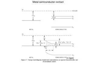
Schottky barriers • Diode like behavior can be mimicked by applying clean metal to a clean semiconductor. • Easy to do and faster switching times can be realized. • n-type • Semiconductor bands bend up causing a more positive region near the interface, which attracts electrons from the metal to the interface interface. • p-type • Semiconductor bands bend down causing a more negative region near the interface, which attracts holes from the metal to the interface.
Rectifying contacts • Apply a forward bias to the Metal of the M/S(n) diode and the contact potential is reduced by Vo-V • Allows electrons to diffuse into metal. • Apply a forward bias to the Semiconductor of the M/S(p) diode and the contact potential is reduced by Vo-V • Allows holes to diffuse into metal.
Rectifying contacts • Apply a reverse bias to the Metal of the M/S(n) diode and the contact potential is increased by Vo+Vr. • Electrons have to overcome a voltage independent barrier to diffuse into metal. • Apply a reverse bias to the Semiconductor of the M/S(p) diode and the contact potential is reduced by Vo+Vr. • Holes have to overcome a voltage independent barrier to diffuse into metal.
Rectifying contacts • Current flows primarily by majority carriers is both cases. • Very little charge storage occurs, which leads to fast switching speeds.
Ohmic contacts • Metal/semiconductor ohmic contacts • linear near the origin, non-rectifying • Two methods of fabrication • Choose a metal with a workfunction that aligns the fermi levels with majority carriers. (Al for p-type Si, Au for n-type Si • Dope the semiconductor heavily so that W is very thin so that tunneling occurs (Al on p+ or n+ Si) • Heavy doping all ways improves ohmic behavior.
Real Schottky barriers • In Si, there is a thin oxide in between the metal and semiconductor. • Surface states arise from the crystal ending • This can pin the fermi level to midgap in GaAs • If a metal semiconductor junction is alloyed the interface is blurred between metal/metal-semiconductor/semiconductor. • Contact design is very dependant on your process.