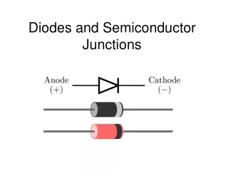
Semiconductor junctions
Semiconductor junctions. And semiconductors. Figure 8.1-1. Band-gap context of semiconductors. . ( a) Donor impurities under E-field (= movement of loose electrons) . ( b) Acceptor impurities under E-field (movement of loose holes) .


Semiconductor junctions
E N D
Presentation Transcript
Semiconductor junctions And semiconductors
(a) Donor impurities under E-field (= movement of loose electrons) (b) Acceptor impurities under E-field (movement of loose holes)
Figure 8.1-3. Holes and electrons analogy to bubblets and pellets.
Figure 8.1-4(a) . The Silicon lattice (diamond lattice unit cell). Figure 8.1-4(b). The array of tetrahedrons along the (110) direction of the crystal.
Figure 8.2-1. Ion implantation process of pnjunction. And a slice across the junction
Figure 8.2-2. Uncovered impurity sites in the vicinity of the pnjunction boundary
(a) I (V) on linear scale. (b) I (V > 0) on logarithmic scale.
Figure 8.3-1. Circuit analysis conductance models of the diode. (A ‘1 mA diode’ is represented)
Figure 8.4-1(a). Series diode and load, also called a half-wave rectifier (HWR). When Vs < 0 the current flow is blocked by the ‘OFF’ state of the diode. Figure 8.4-1(b). Voltage across the load due to IL .
Figure 8.4-2(a). Diode bridge and load, also called a full-wave rectifier (FWR). Figure 8.4-2(b). Voltage across RL due to current through the diodes for the FWR (a.k.a. FWB). Figure 8.4-3 Full-wave rectifier (FWR) topology of figure 8.4-2(a) drawn as a full-wave bridge (FWB). Compare the position of the diodes between this figure and that of figure 8.4-2(a)
Figure 8.4-4. Three-phase sum of rectified currents. The outcome shows up as a steady-state signal with a ripple of peak-peak amplitude VR and frequency = 6 x f0 .
Figure 8.4-5(a). HWR with a capacitance in parallel with the load Figure 8.4-6(a) Outputof HWR with C.
Figure 8.4-5(b). FWR with a capacitance in parallel with the load Figure 8.4-6(b) Output of FWR with C
Figure 8.4-7(a) Zener diode component . When VR exceeds VZ the junction break down. Figure 8.4-7(b) Zener diode I-V response
Figure E8.4-2 Full-wave rectifier AC-DC Zener-regulated charging plug.
DIODE-CAPACITANCE SUBCIRCUIT PRIMITIVES Figure 8.5-1. Peak detector
DIODE-CAPACITANCE SUBCIRCUIT PRIMITIVES Figure 8.5-2. level shifter
Figure 8.5-3. voltage doubler = level shifter followed by peak detector.