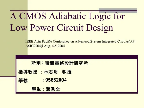
A CMOS Low Power Current-Mode Polyphase Filter
240 likes | 391 Vues
King Fahd University of Petroleum & Minerals KFUPM, Department of Electrical Engineering. A CMOS Low Power Current-Mode Polyphase Filter. By Hussain Alzaher & Noman Tasadduq. OUTLINE. INTRODUCTION Bluetooth receiver Available solutions PROPOSED APPROACH CURRENT AMPLIFIER Introduction

A CMOS Low Power Current-Mode Polyphase Filter
E N D
Presentation Transcript
King Fahd University of Petroleum & Minerals KFUPM, Department of Electrical Engineering A CMOS Low Power Current-Mode Polyphase Filter By Hussain Alzaher & Noman Tasadduq
OUTLINE • INTRODUCTION • Bluetooth receiver • Available solutions • PROPOSED APPROACH • CURRENT AMPLIFIER • Introduction • Fully differential current amplifier (FDCA) • BASIC PRINCIPLE • PROPOSED FILTER • Single ended realization • Fully differential realization • EXPERIMENTAL RESULTS • COMPARISON WITH THE LITERATURE • CONCLUSION
INTRODUCTION • Low-IF Receiver Architecture • Unlike zero-IF: Low-IF = No DC offset and flicker noise problems • Image problem • Solution: Polyphase bandpass filter
INTRODUCTION Available Solutions • Active-RC filters. • High dynamic range. • Limited bandwidth. • Relatively high power consumption. • gm-C filters • High frequency. • Programmable. • Poor linearity=Limited dynamic range.
PROPOSED APPROACH • Design new polyphase filter based on optimum active element • Higher bandwidth than op-amp lower power • Better linearity than gm better DR
PROPOSED APPROACH • Current-mode processing inherently possess • High BW + Low voltage Low Power • High signal swing High linearity • Current Amplifier based Filter • Simple filter topology Low power
CURRENT AMPLIFIER (CA) Introduction • Conveys input current from a low impedance input terminal (X) to a high impedance output terminal (Z). • Gain=K, (sizing of current mirror transistors). • Two types: positive CA (input and output currents are both going in the same direction) and negative CA (having currents in opposite directions). CA with +ve output CA with -ve output
CURRENT AMPLIFIER (CA) Single Input/Dual Output CA Core Input Stage Current Mirrors Class-AB Output Stage
CURRENT AMPLIFIER (CA) Four terminal device, with two input and two output currents. Fully Differential Current Amplifier (FDCA) (Ideally common mode gain is zero) Details available in: H. Alzaher, N. Tasadduq, “Realizations of CMOS fully differential current followers/amplifiers," IEEE International Symposium on Circuits and Systems (ISCAS 2009), pp. 1381-1384.
BASIC PRINCIPLE • General Transfer function • Image Rejection
BASIC PRINCIPLE • Systematic Design • Lowpass filter can be converted to a bandpass polyphase filter centered at ωc. • Complex poles are achieved by using cross-coupling between I and Q paths.
PROPOSED FILTER • Single Ended Realization Simple LP filter to complex filter • Independent control ofωcwithout changing Q using R and/or C.
PROPOSED FILTER • Nominal Values • 6th order polyphase filter is implemented. • The nominal center frequency of 3MHz and overall bandwidth of 1MHz are achieved by selecting R1=13kW, C1=8.5pF and K2=2.1. • K1 is 1 to achieve a gain of unity.
FDCA FDCA PROPOSED FILTER • Fully Differential Realization
PROPOSED FILTER FDCA with four outputs
FOUR OUTPUT CA REALIZATION Core biasing circuit of IB=9mA and ISB=3mA is shared for all FDCA Total biasing current is
EXPERIMENTAL RESULTS • Standard 0.18mm CMOS process. • Supply Voltage ±1.35V. • Total Supply Current 0.88mA. • Center frequency 3MHz. • Bandwidth 1MHz. • Center frequency tuning using capacitor arrays.
EXPERIMENTAL RESULTS • Signal magnitude response showing center frequency tuning
COMPARISON WITH LITERATURE • B. Shi, W. Shan, and P. Andreani, 2002, “A 57dB image band rejection CMOS gm-C polyphase filter with automatic frequency tuning for Bluetooth,” Proc. Int. Symp. Circuits and Systems, ISCAS’ 2002., vol. 5, pp. V-169 - II-172, 2002. • A. Emira, and E. Sánchez-Sinencio, “A pseudo differential complex filter for Bluetooth with frequency tuning,” IEEE Trans. Circuits and Syst.-II, vol. 50, pp. 742 – 754, October 2003. • B. Guthrie, J. Hughes, T. Sayers, and A. Spencer, “A CMOS gyrator Low-IF filter for a dual-mode Bluetooth/ZigBee transceiver,” IEEE J. Solid-State Circuits, vol. 55, no. 9, pp. 1872-1878, Sep. 2005. • C. Psychalinos, “Low-voltage log-domain complex filters,” IEEE Trans. Circuits and Syst.-II, vol. 55, no. 11, pp. 3404- 3412, Dec. 2008.
COMPARISON RESULTS • Power consumption/pole • Proposed filter and [3] • Image rejection • Propsed filter and [2] • SFDR • Proposed filter
CONCLUSION • CA based filters inherently exhibit higher bandwidth than active-RC and better linearity than gm-C. • This is demonstrated by a new polyphase filter with improved SFDR and IRR while using relatively lower power.

