Scanning Tunneling Microscope (STM) and Atomic Force Microscope (AFM)
340 likes | 1.13k Vues
Scanning Tunneling Microscope (STM) and Atomic Force Microscope (AFM). Topographic scan of a glass surface. Types of Microscope. Smaller Scale?. Scanning Probe Microscope. AFM, atomic force microscopy BEEM, ballistic electron emission microscopy CFM, chemical force microscopy

Scanning Tunneling Microscope (STM) and Atomic Force Microscope (AFM)
E N D
Presentation Transcript
Scanning Tunneling Microscope (STM)andAtomic Force Microscope (AFM)
Types of Microscope Smaller Scale?
Scanning Probe Microscope AFM, atomic force microscopy BEEM, ballistic electron emission microscopy CFM, chemical force microscopy C-AFM, conductive atomic force microscopy EFM, electrostatic force microscopy ESTM electrochemical scanning tunneling microscope FMM, force modulation microscopy KPFM, kelvin probe force microscopy MFM, magnetic force microscopy MRFM, magnetic resonance force microscopy NSOM, near-field scanning optical microscopy (or SNOM, scanning near-field optical microscopy) PFM, Piezoresponse Force Microscopy PSTM, photon scanning tunneling microscopy PTMS, photothermal microspectroscopy/microscopy SECM, scanning electrochemical microscopy SCM, scanning capacitance microscopy SGM, scanning gate microscopy SICM, scanning ion-conductance microscopy SPSM spin polarized scanning tunneling microscopy SSRM, scanning spreading resistance microscopy SThM, scanning thermal microscopy STM, scanning tunneling microscopy SVM, scanning voltage microscopy STP, scanning tunneling potentiometry SHPM, scanning Hall probe microscopy SXSTM synchrotron x-ray scanning tunneling microscopy Of these techniques AFM and STM are the most commonly used for roughness measurements
STM • a powerful instrument for imaging surfaces at the atomic level • developed in 1981 • By Gerd Binnig and Heinrich Rohrer (at IBM Zürich), the Nobel Prize winners in Physics in 1986 • 0.1 nm lateral resolution and 0.01 nm depth resolution
electron V2= Vo V1 = 0 A B C V3 = 0 x = -a x = a Quantum Tunneling V e- x Assume the electron has positive energy (E > 0) and E < V2 = Vo. How can the electron tunnel through the energy barrier under the above assumption? Find the wave functions in Region A, B and C respectively to get the answer!
Quantum Tunneling • Write down the Schrodinger’s equations in the 3 regions: 2. Get the general solutions: I, R and T are related to the incident, reflection and transmission coefficients.
Quantum Tunneling Consider only the transmission coefficient: From , we have Tunneling current
Quantum Tunneling From boundary conditions, , for large Ka The thickness a of the energy barrier can be found by measuring the tunneling current!
Operation of STM measure the tunneling current between a conducting tip and conducting sample when a DC bias voltage is applied. Resolution in z (perpendicular to surface) is ~0.01 nm and in x/y is ~0.1 nm, resulting in atomic-resolution images.
L metal 2 metal 1 Operation of STM • Consider two metals, one is a tip and the other is a surface, separated by a finite distance uniform potential barrier. • Electron wave function can tunnel through the barrier and leads to finite current. • The probability is Tunneling current As the two metals move apart, the probability of electrons tunneling decreases exponentially and as they move closer the tunneling increases.
tip Scan direction The current profile duplicates the atomic surface I (nA) x (nm) Operation of STM Constant height Lower current Higher current The air gap (barrier) is several nm Atomic surface
Operation of STM The resolution of bending can be as low as 0.2 nm
The attention paid to the first problem and the engineering solution to it is the difference between a good microscope and a not so good microscope - it need not worry us here, sufficient to say that it is possible to accurately control the relative positions of tip and surface by ensuring good vibrational isolation of the microscope and using sensitive piezoelectric positioning devices. • Tip preparation is a science in itself - having said that, it is largely serendipity which ensures that one atom on the tip is closer to the surface than all others.
Let us look at the region where the tip approaches the surface in greater detail .... ... the end of the tip will almost invariably show a certain amount of structure, with a variety of crystal facets exposed ...
… and if we now go down to the atomic scale .... ... there is a reasonable probability of ending up with a truly atomic tip.
If the tip is biased with respect to the surface by the application of a voltage between them then electrons can tunnel between the two, provided the separation of the tip and surface is sufficiently small - this gives rise to a tunnelling current. • The direction of current flow is determined by the polarity of the bias. If the sample is biased -ve with respect to the tip, then electrons will flow from the surface to the tip as shown above, whilst if the sample is biased +ve with respect to the tip, then electrons will flow from the tip to the surface as shown below.
The name of the technique arises from the quantum mechanical tunnelling-type mechanism by which the electrons can move between the tip and substrate. Quantum mechanical tunnelling permits particles to tunnel through a potential barrier which they could not surmount according to the classical laws of physics - in this case electrons are able to traverse the classically-forbidden region between the two solids as illustrated schematically on the energy diagram below. This is an over-simplistic model of the tunnelling that occurs in STM but it is a useful starting point for understanding how the technique works. In this model, the probability of tunnelling is exponentially-dependent upon the distance of separation between the tip and surface : the tunnelling current is therefore a very sensitive probe of this separation.
Imaging of the surface topology may then be carried out in one of two ways: • in constant height mode (in which the tunnelling current is monitored as the tip is scanned parallel to the surface) • in constant current mode (in which the tunnelling current is maintained constant as the tip is scanned across the surface) If the tip is scanned at what is nominally a constant height above the surface, then there is actually a periodic variation in the separation distance between the tip and surface atoms. At one point the tip will be directly above a surface atom and the tunnelling current will be large whilst at other points the tip will be above hollow sites on the surface and the tunnelling current will be much smaller. A plot of the tunnelling current v's tip position therefore shows a periodic variation which matches that of the surface structure - hence it provides a direct "image" of the surface (and by the time the data has been processed it may even look like a real picture of the surface ! ).
In practice, however, the normal way of imaging the surface is to maintain the tunnelling current constant whilst the tip is scanned across the surface. This is achieved by adjusting the tip's height above the surface so that the tunnelling current does not vary with the lateral tip position. In this mode the tip will move slightly upwards as it passes over a surface atom, and conversely, slightly in towards the surface as it passes over a hollow. The image is then formed by plotting the tip height (strictly, the voltage applied to the z-piezo) v's the lateral tip position.
Piezoelectric Tube • Piezoelectric Material • piezoelectric effect was discovered by Pierre Curie and Jacques Curie • (1880) • An applied mechanical stress will generate a voltage • An applied voltage will change the shape of the solid by a small amount • most well-known piezoelectric material is quartz (SiO2)
Bimorph Two long, thin plates of piezoelectric material are glued together, with a metal film sandwiched in between . Two more metal films cover the outer surfaces . Both piezoelectric plates are poled along the same direction, perpendicular to the large surface By applying a voltage, stress of opposite sign is developed in both plates, which generates a torque
Making a sharp tip • By electrochemical etching method Consider a gold tip prepared in 0.8 M KCN solution from a gold wire (Au), the following electrochemical redox reaction takes place:4Au(s)+8KCN(aq)+O2(g)+2H2O→ 4Au(CN)2−(aq)+4OH−(aq)+8K+(aq) By applying different voltages, some part of tip were washed with the distilled water
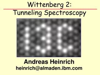
Lithography and micromanipulation • The interactions between the STM tip and substrate can be used to modify the surface in a controlled way. • This can be done in a number of ways. • Eg Eigler and Schweizer manipulated xenon atoms on a Nickel(110) surface under UHV conditions, with everything at 4K. • They reported that under these conditions everything was stable for days. • This allowed them to move single atoms at a time until they achieved the following result.
