
SlideServe
Menu
Préférences
© SlideServe · v2026

High-Resolution Imaging in Ultra-Low Vibration Lab Designs

sai avatar
1 diapositives · 151 Views · Aug 22, 2014

Explore tunneling currents, differential conductance, and local density of electronic states in advanced lab settings with cutting-edge STM technology. Witness groundbreaking studies on cuprate and semiconductor materials.
High-Resolution Imaging in Ultra-Low Vibration Lab Designs - slide 1
01 / 1High-Resolution Imaging in Ultra-Low Vibration Lab Designs
1 / 17

Télécharger la présentation

High-Resolution Imaging in Ultra-Low Vibration Lab Designs
Une image / un lien ci-dessous est fourni (tel quel) pour télécharger la présentation

Politique de téléchargement : le contenu du site vous est fourni TEL QUEL pour votre information et votre usage personnel ; il ne peut être vendu, concédé sous licence ni partagé sur d’autres sites sans l’accord de son auteur.Le contenu vous est fourni TEL QUEL, pour votre information et votre usage personnel uniquement. Téléchargez la présentation en cliquant sur ce lien. Lors du téléchargement, si vous ne parvenez pas à télécharger une présentation, l’éditeur a peut-être supprimé le fichier de son serveur.Pendant le téléchargement, si vous ne parvenez pas à obtenir une présentation, le fichier a peut-être été supprimé par l’éditeur.

F I N

Plus de contenu associé

Transcription de la présentation
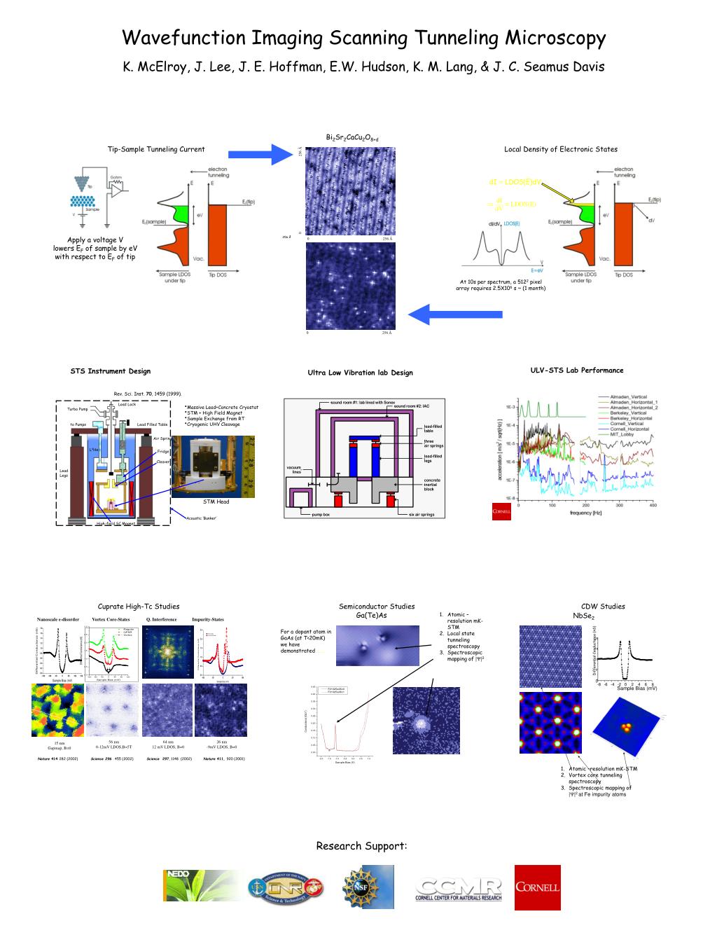
  1. ULV-STS Lab Performance Tip-Sample Tunneling Current 20 2500 Å 15 Differential Conductance (nS) 10 3.75” sq. at 5.8”, 2” 5 Apply a voltage V lowers EF of sample by eV with respect to EF of tip 0 Å 0 Å 2500 Å 0 -8 -6 -4 -2 0 2 4 6 8 Sample Bias (mV) Wavefunction Imaging Scanning Tunneling Microscopy K. McElroy, J. Lee, J. E. Hoffman, E.W. Hudson, K. M. Lang, & J. C. Seamus Davis Bi2Sr2CaCu2O8+d Local Density of Electronic States 0 256 Å 5.5” sq at 1.5”, 2.75” 91114I02 256 Å 0 256 Å 91119c01 +10mV At 10s per spectrum, a 5122 pixel array requires 2.5X10⁶ s ~ (1 month) 0 256 Å STS Instrument Design Ultra Low Vibration lab Design Rev. Sci. Inst. 70, 1459 (1999). Load Lock • Massive Lead+Concrete Cryostat • STM + High Field Magnet • Sample Exchange from RT • Cryogenic UHV Cleavage Turbo Pump to Pumps Lead Filled Table Air Springs L4He Fridge Cleaver Lead Legs STM Head Acoustic ‘Bunker’ High-field SC Magnet Cuprate High-Tc Studies Semiconductor Studies CDW Studies Ga(Te)As • Atomic –resolution mK-STM • Local state tunneling spectroscopy • Spectroscopic mapping of |Y|2 NbSe2 Nanoscale e-disorder Vortex Core-States Q. Interference Impurity-States For a dopant atom in GaAs (at T<20mK) we have demonstrated ……. 128 Å 56 nm 0-12mV LDOS,B=5T 64 nm 12 mV LDOS, B=0 26 nm -9mV LDOS, B=0 15 nm Gapmap, B=0 Nature 414 282 (2002) Science 296455 (2002) Science 297, 1148 (2002) Nature 411, 920 (2001) • Atomic –resolution mK-STM • Vortex core tunneling spectroscopy • Spectroscopic mapping of |Y|2 at Fe impurity atoms Research Support: