Scanning Tunneling Microscopy STM
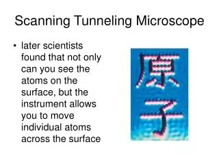
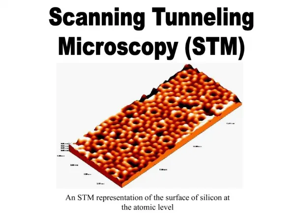
What is Scanning Tunneling Microscopy?. Allows for the imaging of the surfaces of metals and semiconductors at the atomic level.. . Developed by Gerd Binnig and Heinrich Rohrer at the IBM Zurich Research Laboratory in 1982.. . . The two shared half of the 1986 Nobel Prize in physics for developing STM..

Scanning Tunneling Microscopy STM
E N D
Presentation Transcript
3. Stylus Profiler (1929 �Schmalz)
4. Topographiner (1971 �Young)
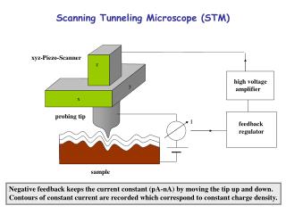
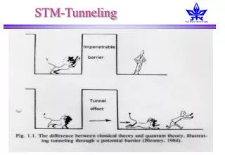
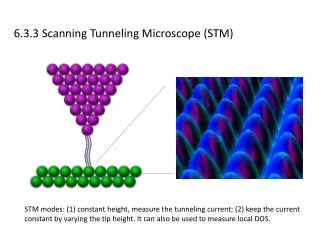
5. STM
14. Since you are measuring the electronic states, images of the same surface can vary!
15. Graphite is a good example! STM images of graphite
22. Question: At low voltages and temperature the tunneling current is given by:
where d is the distance between the tip and sample, K is the decay constant, m is the mass of an electron, ? is the barrier height and h is planks constant. Assume the local barrier height is about 4eV. Show the current sensitivity to distance between the tip and sample if the current is kept within 2%.
23. Answer
24. Question Bias-dependent STM images can probe the occupied and unoccupied states. Here are the STM images of GaAs(110)-2x1surface. Images were obtained by applying (a) +1.9V (b) -1.9V to the sample wtih respect to the tip. The rectangles in the images indicate the corresponding position. And it was suggested that the filled states are localized on the As atoms, while the empty states are localized on the Ga atoms. Draw the GaAs(110)-2x1 surface. and gives a little explanation as well.
25. Answer When the sample is biased positive, electrons from occupied states of the tip tunnel to the unoccupied states of the sample, so image (a) (see question) represents the Ga states, while image (b) (see question) represents As states. The position of surface atoms are schemiatically shown in picture (c), where small dots indicate As atoms and large dots represent Ga atoms.