Download

1 / 13
230 likes | 786 Vues
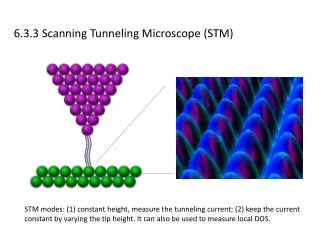
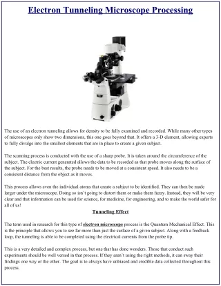
Introduction to scanning tunneling Microscope (STM). Chien -Chang Chen ( Nai -Chang Yeh’s group). Image from an STM. Image from an STM. Iron atoms on the surface of Cu(111). STM schematic.

E N D
Introduction to scanning tunneling Microscope (STM) Chien-Chang Chen (Nai-Chang Yeh’s group)
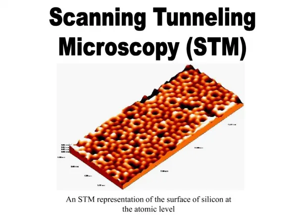
Image from an STM Image from an STM Iron atoms on the surface of Cu(111)
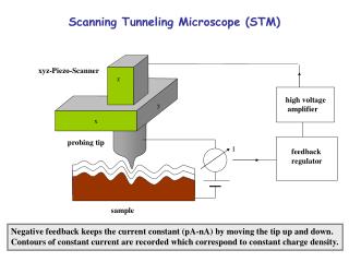
STM schematic "ScanningTunnelingMicroscope schematic" by Michael Schmid - Michael Schmid, TU Wien; adapted from the IAP/TU Wien STM Gallery. Licensed under Creative Commons Attribution-Share Alike 2.0-at via Wikimedia Commons - http://commons.wikimedia.org/wiki/File:ScanningTunnelingMicroscope_schematic.png#mediaviewer/File:ScanningTunnelingMicroscope_schematic.png
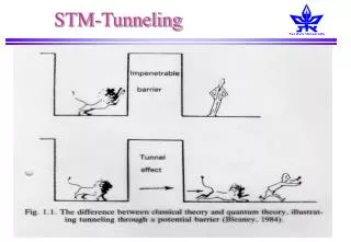
Theory of STM: tunneling effect , from WKB approximation
Tunneling current • , where , is the work function • With unit, • For most metal (Au 5.4eV; Pt 5.7eV; Ir 5.6eV), , • That means current decay about 10 time per • The distance between atoms is more than 1 . Atomic resolution can be achieved if tip is good enough.
thanks to http://www.toutestquantique.fr Video: tunneling effect
Tunneling current with bias is the Fermi distribution is the energy state at tip and sample (to Fermi level) , tunneling matrix and are the density of state for tip and sample
A little more approximation • step function • If the tip is metal. around Fermi energy • Thus, by calculating the derivative of tunneling current versus voltage, we can get the density state of sample
What STM can really detect • STM detect the electronic state, not the atom itself. • We can detect different electronic state or even bonding by applying different voltage
The operation of STM • Constant current mode use the feedback to maintain the tip at constant density of state position. If the material is the same, this can be seen as constant distance from the sample. Thus we can get the topography image of the sample surface • Constant height mode disable the feedback and let tip move in the constant height. The scan in this mode can be much faster, but can only be done in the flat surface to avoid the crash of the tip
Positioning • The STM tip position was controlled by several piezoelectrical component • For the ease of use, it usually includes coarse positioner and fine positioner (tube scanner with tip)
Conclusion • STM and (AFM) make seeing atom and manipulate the atom not a dream at all. • We can control and play the single atom. Someone even draw a movie by atoms • STM gives us the direct and extremely localized information about electronic density of state for the materials. Even the spin can be measured by the spin-polarized STM. • STM is suitable to study the material with non-empty density of state, that is metal, semiconductor • With AFM, even the insulator can be studied directly