New Research Using a Scanning Tunneling Microscope (STM)
220 likes | 532 Vues
New Research Using a Scanning Tunneling Microscope (STM). Ian Schwartz. Agenda. Introduction: Moore’s Law and an overview of various competing research topics for future CMOS technology About the Scanning Tunneling Microscope (STM) STM & The Future

New Research Using a Scanning Tunneling Microscope (STM)
E N D
Presentation Transcript
New Research Using a Scanning Tunneling Microscope (STM) Ian Schwartz 18-610
Agenda • Introduction: Moore’s Law and an overview of various competing research topics for future CMOS technology • About the Scanning Tunneling Microscope (STM) • STM & The Future “IBM scientists can now measure how long information can stay in an individual atom, getting one step closer to the goal of computing at the atomic level.” --eWeek.com 18-610
Silicon 3-Dimensional FinFET http://postreh.com/vmichal/thesis/figures/figures.htm • Currently the smallest technology with a channel length of 3 nm http://tr.ietejournals.org/article.asp?issn=0256-4602%3Byear=2010%3Bvolume=27%3Bissue=6%3Bspage=446%3Bepage=454%3Baulast=Subramanian Current CMOS technology Projected minimum gate length of 6 nm (but will be hindered by quantum tunnelling) 18-610
Ge, III-V http://www.ims.demokritos.gr/DUALLOGIC/ Graphene • Fast and stable, but cannot reach a very small channel length compared to the molecular level http://www.physorg.com/news178552799.html Estimated minimum size of 10 nm 18-610
Single-Walled Nanotubes http://jnm.snmjournals.org/cgi/content/full/48/7/1039/FIG1 Single-Electron Transistor Adit Gupta, Sandeep Kotak, Ana MartinezMarrosu, Erik Stegall University of Buffalo (left) • Minimum channel length of 10 nm http://en.wikipedia.org/wiki/Coulomb_blockade (right) Molecular Electronics/Spintronics • Memory, data processing, and communication can be accomplished using a single atom 2-D graphene structure Can be used for wires or transistors 1-2 nm diameter 18-610
Moore’s Law http://www.tf.uni-kiel.de/matwis/amat/elmat_en/kap_5/illustr/i5_4_1.html 18-610
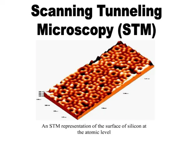
http://www.uta.edu/engineering/nano/facility.php?id=55&cat2=STMhttp://www.uta.edu/engineering/nano/facility.php?id=55&cat2=STM 18-610
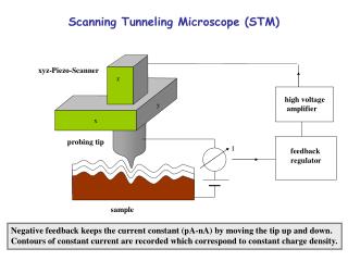
Operation of the STM http://rxinspector.com/scanning-tunneling-microscope-picture/ 18-610
Operation of the STM http://www.ipp.mpg.de/ippcms/eng/for/bereiche/material/projekte/pww/oplab.html http://www.science.psu.edu/news-and-events/2005-news/Weiss12-2005.htm 18-610
New STM Technology • At first, the STM was used only as a microscope • Later the STM was used for growing and etching epitaxial layers and structures at the atomic level • The new innovation discussed next allows the user to use the STM as a video camera 18-610
New STM Technology • This new method is accomplished by using the STM stroboscopically • “Pump-probe” measurement technique: • A single, quick voltage pulse (pump pulse) is applied across the tunnel junction to excite the atom • Then a weaker pulse (probe pulse) is applied to measure the state of the atom’s spin at a time Δt after the pump pulse • This is one “frame” • Integrating this current over many pump-pulse cycles with a varying Δt creates a moving image of the atom’s spin 18-610
New STM Technology • The tunnel junction conductance varies corresponding to the alignment of the sample’s spin with the tip’s spin • A series of voltages Vpump and Vprobe are sent to the tip • The integral of the probe-pulse current as a function of the delay time between pulses (Δt) yields the spin cycle of the atom http://www.sciencemag.org/content/329/5999/1628.full 18-610
New STM Technology • Previously, atoms could only be tracked in increments of milliseconds • This new technique using the STM allows the user to follow the movement of an atom in increments of nanoseconds • This adds a new dimension, time, to experiments at the atomic level 18-610
Uses and Discoveries • Scientists at IBM can now measure an atom’s magnetic orientation with respect to time (electron spin relaxation time) • This led to the discovery of the threshold voltage value Vthr of an Fe-Cu bond, which is 16.7 mV http://www.sciencemag.org/content/329/5999/1628.full 18-610
Uses and Discoveries • Figure (A) above shows the number of electrons per pulse with respect to the delay time for three different B values • Figure (B) shows the relaxation time versus magnetic field for two different Fe-Cu atom configurations • This led to the discovery that an atom can hold its memory for up to 200 nanoseconds. Scientists previously believed this number was just 1 nanosecond http://www.sciencemag.org/content/329/5999/1628.full 18-610
STM and the Future • Goal: to manipulate an atom’s storage time from nanoseconds to hours or days • Could take between two and five years to finish research on this subject • Up to 15 years or more to determine if this research can result in production 18-610
My Opinion? I suggest the following strategy (though I know nothing about the business aspect…!): Continue minimizing the Si technology. However, decrease the amount of research on this area, and slowly increase the research towards the manipulation of the electron relaxation time in an atom. If we put all of our energy into this technology and succeed, we as a human race can say that we have successfully beaten semiconductors! However, if we fail or take too long to accomplish this, businesses would start to crumble and the entire economy of the world may crash. 18-610
"Jumping to the scale of a single atom, that is clearly at the end of the road map." --Andreas Heinrich, group leader of nanoscale science at IBM 18-610