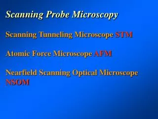
Scanning Tunneling Microscope (STM)
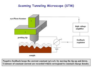
Scanning Tunneling Microscope (STM). xyz-Piezo-Scanner. z. high voltage amplifier. y. x. probing tip. feedback regulator. I. sample. Negative feedback keeps the current constant (pA-nA) by moving the tip up and down.

Scanning Tunneling Microscope (STM)
E N D
Presentation Transcript
Scanning Tunneling Microscope (STM) xyz-Piezo-Scanner z high voltage amplifier y x probing tip feedbackregulator I sample Negative feedback keeps the current constant (pA-nA) by moving the tip up and down. Contours of constant current are recorded which correspond to constant charge density.
Technology Required for a STM • Sharp, clean tip (Etching, ion bombardment, field desorption by pulsing) • Piezo-electric scanner (Tube scanner, xyz scanner) • Coarse approach (Micrometer screws, stick-slip motors) • Vibrational damping (Spring suspension with eddy current damping, viton stack) • Feed-back electronics (Amplify the current difference, negative feedback to the z-piezo)
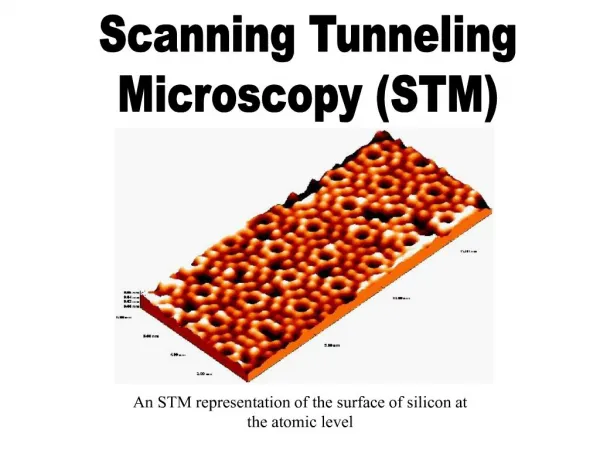
Usually, only one atom at the end of the tip carries most of the current. This is the atom that sticks out the most. (Remember the factor 100 decrease in the tunneling current per atom diameter.) The atom at the end of the tip compares to a ping-pong ball at the top of the Matterhorn. (The STM was invented in Switzerland!)
L Piezoelectric effect A piezoelectric material changes its length when an electric field is applied. Vice versa, it generates an electric field when squeezed or expanded. The analog to piezoelectricityin magnetism is called magnetostriction. It is produces unwanted magnetic fields in strained nanomagnets. Piezoelectric scanners work with the transverse piezoelectric effect. The crystal is elongated perpendicular to the applied electric field. L Eelectric field, L length, L elongation, d31 transverse piezoelectric coefficient E A typical material is PZT (lead zirconium titanate). The ratio between lead and zirconium determines the Curie-temperature and the piezoelectric coefficient. Example: PZT-5H: d31 = -2.62Å/V i.e. L=1 cm, L = 1 m, E=380 V/mm
Piezoelectric scanners For three-dimensional positioning one uses xyz-leg scanners or tube scanners. The tube scanner is more compact (vibrates less, more sturdy). Its sensitivity is: V: applied voltage, L length, H thickness, d31 transverse piezoelectric coefficient.
Coarse approach • Surprisingly, this has been one of the most difficult obstacles in getting STM going. Think of the problem the following way: One starts out with the tip about a milli-meter away from the sample and has to get within about a nanometer to get the tunneling current started. That is a factor of a million. It is like driving 1000 kilo-meters and stopping from full speed to zero within a meter. That might be possible going very slowly in a car with good brakes, but it would take days (weeks?). • These days the tip approach is automated and run by a computer program. One uses two z-motions, a stick-slip motor with coarse motion and a z-piezo for the fine approach. The following two steps are repeated over and over again: • Expand the z-piezo fully while checking for tunneling current. • If no current is detected, retract the z-piezo all the way and move the coarse motor. • Eventually, a tunneling current will be detected and the loop stops.
Feedback regulator - + z How does one keep the tunneling current I constant in STM? The current is compared to a reference current I0 (typically 0.1 nanoampere). The difference (I-I0) is amplified by a factor P and converted into a voltage for the z-piezo (typically 100V). The sign is important to make sure that the tip moves away if the current too high, thereby reducing it (negative feedback). In addition to this linear feedback (proportional to I-I0)one can use the time integral over (I-I0), as shown in the lower branch of the diagram. This produces long-term stability and prevents feedback oscillations. One can also use the time derivative of (I-I0) as feedback in order to increase the scanning speed. By itself the derivative is prone to oscillations, but it can be stabilized by combining it with an integral feedback.
Vibration damping The key to vibration damping is to keep the resonance frequency 0 of the STM as low as possible (typically 1 Hz). This way most other vibrations are so far above resonance that they couple very little. The main problem is low-frequency noise (for example from air conditioning fans). One can try to calculate all of this (see below), but it is faster to hook up a spectrum analyzer to the tip height signal to find the sources of vibrations. STM (0’ , Q’) Transfer function of the STM Damped table (0 , Q) Total transfer function: TT =T ·TS Transfer function of the table
Atomic Force Microscope (AFM) deflection sensor cantilever feedbackregulator probing tip sample high voltage amplifier xy-piezo (lateral position) z-piezo (tip-sample distance) Negative feedback keeps the force constant by adjusting the z-piezo such that the up-down bending angle of the thin cantilever remains constant.
Deflection sensors Photodiode with four quadrants Laser
Beam-deflection method A light beam is reflected from the cantilever onto a photodiode divided into 4 segments. The vertical difference signal provides the perpendicular deflection. The horizontal difference signal provides the torsional bending of the cantilever. The two deflections determine perpendicular and lateral forces simultaneously.
40 m AFM Cantilever and TipTo obtain an extra sharp AFM tip one can attach a carbon nanotube to a regular, micromachined silicon tip.
Principle of AFM F U z repulsive attractive Energy Uand force Fbetween tip and sample as a function of their distance z. The force is the derivative (= slope) of the energy. It is attractive at large distances (van der Waals force, non-contact mode), but it becomes highly repulsive when the electron clouds of tip and sample overlap (Pauli repulsion, contact mode). In AFM the force is kept constant, while in STM the current is kept constant.
Dynamic Force Detection The cantilever oscillates like a tuning fork at resonance. Frequency shift and amplitude change are measured for detecting the force. (a) High Q-factor = low damping (in vacuum): Sharp resonance, detect frequency change, non-contact mode (b) Low Q-factor = high damping (in air, liquid): Amplitude response, detect amplitude change, tapping mode
STM versus AFM STM is particularly useful for probing electrons at surfaces, for example the electron waves in quantum corrals or the energy levels of the electrons in dangling bonds and surface molecules.AFM is needed for insulating samples. Since most polymers and biomolecules are insulating, the probe of choice for soft matter is often AFM. This image shows DNA on mica, an insulator.
(S)TEM (Scanning) Transmission Electron Microscopy Atomic resolution image of atom columns in Si (aberration corrected) Diffraction pattern: Higher order spots improve the resolution. Conventional Aberration corrected Batson, Dellby, Krivanek, Nature 418, 617 (2002). Z contrast at an interface
Identify Elements by EELS (Electron Energy Loss Spectroscopy) An element can be identified by its characteristic energy losses via excitation of core levels. The same transitions as seen by X-ray absorption spectroscopy.
Identify Elements by EDX (Energy-Dispersive X-ray Analysis) Identify an element by its core level fluorescence energy. Semiconductor Si(Li) Detector An X-ray photon creates many electron-hole pairs in silicon, whose number is proportional to the ratio between photon energy hand band gap EG : h/EG keV / eV 103 Pulse height proportional h