Chapter 10. Phase-Locked Loops
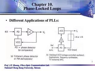
Chapter 10. Phase-Locked Loops. Different Applications of PLLs:. Phase-Locked Loop Applications. Phase-Locked Loop Applications. Figure 10-1. Phase-locked loop applications. The Phase Detector.

Chapter 10. Phase-Locked Loops
E N D
Presentation Transcript
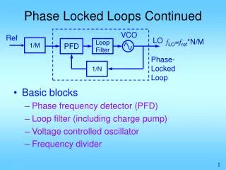
Chapter 10.Phase-Locked Loops • Different Applications of PLLs:
Phase-Locked Loop Applications Figure 10-1. Phase-locked loop applications.
The Phase Detector • A simple analog phase detector is shown in Figure 10-2a. Consider the phase detector as a simple switch, as illustrated in Figure 10-2b. • The signal with frequency fo simply opens and closes the (diode) switch. If fi ≠ fo, then the circuit behavior is that of a mixer producing the sum and difference frequencies.
The Phase Detector • The capacitors shown are chosen to bypass fi, fo, and fi + fo, and therefore only the beat (fi - fo) signal is seen at vd. After the loop is locked, fo will be exactly equal to fi. • A phase difference between the two input signals results in a dc voltage Vd, which is proportional to the phase difference, qe = qi - qo .
The Phase Detector Figure 10-2. (a) Analog phase detector. (b) Simpified model.
The Phase Detector • A mixer performs the mathematical function of multiplication. Thus for sinusoidal inputs, • When phase-locked, wo = wi, the second harmonic term, Asin[2wot + qo + qi], is filtered out, leaving Vd = Asin(qi - qo) (10-1) • This voltage is directly proportional to the input signal amplitude and the phase error qe if the signal amplitude is held constant. • Indeed, for small qe , this transfer function is linear as seen in Figure 10-3.
The Phase Detector Figure 10-3. Analog phase detector characteristic-output voltage versus input phase difference.
The Phase Detector Figure 10-4. Phase detector waveforms.
The Phase Detector • Figure 10-4 helps to show the results graphically as oscilloscope measurements. • When the signals are out of phase by 90o as in part (a), a zero dc output results; • If the phase is slightly advanced as in part phase as in part (b), a small negative dc output is produced; • When the signals are exactly in phase as in part (c), the result is a dc output proportional to the fi signal level--exactly the kind of signal that is needed for a lock indication in telephone touchtone decoders or AGC in coherent receivers.
Phase Detector Gain • The PD characteristic is a continuous sinusoid repeating every 2p radians. Also, during the tracking mode, operation is limited to the portion of the curve between +p/2 where |qe| < p/2. • For sinusoidal inputs it is clear from Figure 10-6 that the slope of the phase detector characteristic curve, Vd = Asinqe (10-2)is not constant. • In fact, it rises with a maximum slope at qe = 0, and levels off to a slope of zero (no gain) at qe = p/2 radians.
Phase Detector Gain • The peak voltage A is the volts-per-radian gain of this phase detector because the tangents to the peak and the PD curve at qe = 0 intersect at one radian, as seen in Figure 10-6. • Therefore the gain of the analog phase detector is kf = A (volts/radian) (10-3)
Phase Detector Gain Figure 10-6. Sinusoidal characteristic of analog phase detector.
Phase Detector Gain • If the input signals are both square-waves, the phase detector characteristic will be linear, as illustrated in Figure 10-7. • The gain of this circuit is constant over the range of input qe = +p/2 and is given by kf = Vd/qe = A/(p/2). • That is, kf = 2A/p (volts/radian) (10-4)
Phase Detector Gain Figure 10-7. Phase comparator characteristic for square-wave inputs.
Phase Detector Gain • Figure 10-8 is typical of balanced integrated circuit implementations. This circuit is also used as a balanced AM modulator for producing double-sideband/suppressed-carrier signals and consists of differential amplifiers. • The oscillator input polarity determines which differential pair conducts, while the signal input determines whether Rc1 or Rc2 receives the current. • The output voltage will be the difference between i1Rc1 and i2Rc2 .
Phase Detector Gain Figure 10-8 Integrated circuit balanced detector.
Digital Phase (Timing) Comparators • Digital phase detectors can be realized using an exclusive-OR (Figure 10-9) or an edge-triggered set-reset flip-flop (RS-FF) circuit. • The exclusive-OR output Y is low when both inputs are high or low; otherwise Y is high, indicating “or.” • The output is smoothed (integrated) to produce Vd. The exclusive-OR requires symmetrical square wave inputs, • which may become a system problem, whereas the edge-triggered RS-FF works well with pulses.
Digital Phase (Timing) Comparators Figure 10-9. Digital implementation of phase detector using an exclusive-OR gate.
Digital Phase (Timing) Comparators • As illustrated for the circuit of Figure 10-10, the RS-FF phase detector can produce a linear PLL over a full qe range of 2p rad, which is twice that for the other phase detectors. • The problem with using digital phase detectors in sensitive communication receiver applications is in the difficulty of filtering the sharp impulses and their harmonics to prevent radio-frequency interference (RFI).
Digital Phase (Timing) Comparators Figure 10-10. Digital implementation of phase detector using a set-reset flip-flop.
Amplifiers Figure 10-11. Operational amplifiers increase PLL loop gain.
Amplifiers • The second loop component is an amplifier commonly referred to as the dc amp. Its function is to increase the loop gain by amplifying the phase detector output voltage. • Figure 10-11 shows three voltage amplifiers and their gain parameter kA = AV (volts out/volts in). • The bandwidth of the dc amp must be very high compared to the loop bandwidth or loop instability will result--even to the point of oscillation due to excessive phase shift around the loop, which would produce positive (regenerative) feedback.
Voltage-Controlled Oscillator (VCO) Figure 10-12. Tuning diode control of free-running multivibrator.
Voltage-Controlled Oscillator (VCO) • The frequency of the free-running multi-vibrator circuit of Figure 10-12 is controlled by the variable reactance of D1 and D2. In IC implementations, D1 and D2 are realized by reverse-biased collector junctions. • It should be noted that the control voltage must not exceed VE + 0.5V + ve, where ve is the positive peak of the oscillator signal across RE and 0.5V causes forward bias of the silicon diodes.The input-output characteristic for the VCO is shown in Figure 10-13.
Voltage-Controlled Oscillator (VCO) Figure 10-13. VCO characteristic.
BASIC LOOP BEHAVIOR- Locking the loop • Start with switch open (Figure 10-14) and a signal generator with frequency fi connected to the input. • With fi not equal to the free-running frequency (fFR), the phase detector will produce the sum and difference frequencies. • The loop (low-pass) filter filters out the sum frequency (fi + fFR), fi , and fFR, while the difference (fi - fFR)--the beat between the signal generator and VCO--is allowed to pass through. • The beat is amplified and seen as on an oscilloscope. As the generator frequency is varied to bring fi closer to fFR, the beat frequency gets lower and lower. This is illustrated in Figure 10-15.
BASIC LOOP BEHAVIOR- Locking the loop Figure 10-14. PLL block diagram.
BASIC LOOP BEHAVIOR- Locking the loop Figure 10-15. Beat-frequency output at Vo with loop open. The input generator frequency is being varied from fi < fFR to fi > fFR.
Acquisition • In Fig. 10-14, with the VCO input grounded and Vo = 0, measurements will show that fi= fFR. • However, if fi≠fFR, then the beat is observed at Vo. When the switch is closed, the beat-frequency signal at Vo will cause the VCO frequency fo to change. • If the voltage is large enough (high loop gain) and the filter bandwidth wide enough, then the VCO will be deviated from fFR and lock at the instant that fo = fi .
Acquisition • The amount by which the VCO frequency must be changed is Df = fi - fFR. The time required for the loop to lock depends on the type of loop and loop dynamics. • For the simplest PLL with no loop filter, this acquisition time is on the order of 1/kv seconds. • Also, the range of fi over which the loop will lock, the lock range, is equal to the hold-in range for the simple PLL.
Locked Loop: The Tracking Mode • When the loop is locked we know that fo = fi. Only a phase difference between the signal and the VCO can exist. • This phase difference qe = qi - qo is called the static (dc) phase error. • qe is the input to the phase detector when the loop is locked and is required in order for the phase detector to produce a dc output voltage Vd . • The dc output voltage Vd, when amplified by the dc amplifier, will produce exactly enough Vo to keep the VCO frequency deviated by Df.
Locked Loop: The Tracking Mode • If fi increases, then Df increases and qe must increase in order to provide for more Vo to keep the VCO tracking fi. • The definition of locked is that fi = fo and the loop will track any change in fi. • Any subsequent shift of qi or qo will be tracked-out so that only qe remains.
Hold-In Range • The range of frequencies for fi over which the loop can maintain lock is called hold-in range. • Assuming that the amplifier does not saturate and the VCO has a wide frequency range, the phase detector characteristic limits the hold-in range. • It should be clear from the phase detector characteristics (Figs 10-6 and 10-7) that, as the static phase error increases due to increasing fi , a limit for Vd is reached beyond which the phase detector cannot supply more voltage for VCO correction.
Hold-In Range • The phase detector simply cannot produce more than A volts. The total range of Vd is ±A= 2A, so that the total range of qe is p radians. • From Equ. (10-7), the minimum to maximum input frequency range, fi(max) - fi(min) = DfH, will be DfH = pkL or DfH = kv/2 (10-9) • The edge-triggered R-S flipflop phase comparator of Figure 10-9 can provide twice this, DfH = kv.
Loop Gain and Static Phase Error • The locked PLL is seen in Figure 10-16. The phase comparator develops an output voltage Vd in response to a phase difference between the reference input and the VCO. • The transfer gain kf has units of volts/radian of phase difference. The amplifier shown is wideband with a voltage gain of kA volts/volt (dimensionless). Thus, Vo= kAVd.
Loop Gain and Static Phase Error Figure 10-16. PLL in tracking mode (locked).
Loop Gain and Static Phase Error • The VCO free-running frequency is fFR. The VCO frequency fo will change in response to an input voltage change. • The transfer gain ko has units of kHz/V. The loop gain for this system is simply the gain of each block multiplied around the loop, • thus kL = kf.kA.ko (10-6) The units of kL are (V/rad).(V/V).(kHz/V) = kHz/rad.
Loop Gain and Static Phase Error • Assume that a signal with frequency fi is an input to the phase detector, and the loop is locked. • If the frequency difference before lock was Df= fi - fER, then a voltage Vo=Df/ko is required to keep the VCO frequency equal to fi. • So the phase comparator must produce Vd = Vo/kA = Df/kAko, and the static phase error qe = qi - qo must be qe = Vd/kf.
Loop Gain and Static Phase Error • Combining gives qe = Df/ kfkAko = Df/kL. This is a fundamental equation for the PLL in phase lock; qe = Df / kL. (10-7) • In many computations the loop gain must be in units of rad/sec rather than in kHz/rad. The conversion is made using 2p radians/cycle. • Hence, loop gain is also given by kv = 2pkfkAko (10-8) in unit of sec-1 or radians/second.
Loop Gain and Static Phase Error • Example: Figure 10-17 provides enough information to analyze the static behavior of a phase-locked loop. 1. Determine kA for the op-amp. 2. Calculate the loop gain in units of sec-1 and in dB (at w = 1 rad/s). 3. With S1 open as shown, what is observed at Vo with an oscilloscope? 4. When the loop is closed and phase-locked, determine (a) the VCO output frequency, (b) static phase error at phase comparator output, (c) Vo (is this rms, pk-pk, or what?). 5. Determine the hold-in range DfH. 6. Determine A, the maximum value of Vd.
Loop Gain and Static Phase Error Figure 10-17. Example PLL.
Loop Gain and Static Phase Error Solution: 1. kA = (Rf/R1) + 1 = 4kW/1kW + 1 = 5. 2. kL = kfkAko = 0.1 V/rad x 5 x (-30 kHz/V) = -15x103 (Hz/rad). Then, kv = 15x103cycles/s-rad x (2p rad/cycle) = 94300 sec-1, and kv(dB) = 20 log kv = 20.log(94.3x10³) = 99.5dB at 1 rad/s. 3. Vo will be a sinusoidally varying voltage with a frequency of |fi–fFR| = 10 kHz. This assumes that a very small capacitor internal to the phase comparator filters out fo, fiand fo+fi.
Loop Gain and Static Phase Error 4(a). When the loop is locked, fo = fi= 100 kHz by definition of locked, and only a phase difference can exist between the input signal and VCO. This phase difference qe is the loop-error signal (static phase error) which results in Vd at the detector output and, when amplified bykA, provides enough voltage Vo to make the VCO frequency be exactly equal to fi.
Loop Gain and Static Phase Error 4(b). The free-running frequency of the VCO is 110 kHz. In order for the VCO to equal 100 kHz, the VCO input voltage must be Vo = (100 kHz –110 kHz)/ko = 10 kHz/(-30 kHz/V) = 0.33Vdc. Then, because kA= 5, Vd must be Vd= 0.33V/5 = 0.0667V. Finally, qe = Vd/kf = 0.0667V/0.1V/rad = 0.667 rad. Once again, we have derived the basic relationship, qe = Df/kL = (fi - fER)/kL = -10 kHz/(15x103 Hz/rad) = 0.667 rad.
Loop Gain and Static Phase Error 4(c). The input to the phase detector (loop-locked)was determined from qe = Df/kL = 0.667 rad. Since Vd = kf qe, we have Vd = 0.1 V/rad x 0.667 rad = 0.0667 Vdc. Assume that Zin of the op-amp is >> R of the loop filter, so there is no voltage drop across R. The input to the op-amp is 0.0667 Vdc, so that Vo= kAVd = 5 ×0.0667 Vdc = 0.33 Vdc. This is enough to keep the VCO at 100 kHz when in fact its rest frequency is 110 kHz.
Loop Gain and Static Phase Error 5. When the loop is locked, how much can fi change in frequency before the loop just cannot provide enough Vo to keep the VCO at fo = fi? Assuming that the VCO and dc amplifier don't saturate, we look at the phase detector characteristic. Clearly Vd can increase with qe until Vd --> Vmax = A, at which point qe = p/2 . Beyond this, Vd decreases for increasing static phase error, and the phase detector simply cannot provide more output voltage to continue increasing fo, and the loop breaks lock. The total hold-in range is +p/2, or p rad. The frequency difference between these break-lock points will be DfH = qe(max) x kL = p x 15 kHz/rad = 47.1 kHz.
Loop Gain and Static Phase Error 6. At the frequency where qe = p/2, we have Vd(max) = A. Therefore Vd = kfqe = 0.1 V/rad × p/2 rad = 0. 157 Vdc
FM and FSK Applications of PLLs • When a PLL has locked to an input signal, the VCO will follow slow changes in the input signal frequency fi. • Suppose fi increases by an amount Dfi. In order for the loop to remain locked (fo - fi), the VCO voltage must increase by DVo = Dfi/ko. • This voltage change is produced by the amplified change in Vd, which is produced by an increased phase difference, Dqe = 2pDfi/kv.
FM and FSK Applications of PLLs • As a specific example, suppose that an FM signal with carrier frequency fi is modulated to an index of mf= 4 by a 1-kHz sinusoid. • The carrier frequency will be deviated above and below fi by an amount Dfi = mffm = 4 x 1 kHz = 4 kHz pk. • If this FM signal is the input to a PLL with a VCO gain of ko = 10 kHz/V and loop bandwidth 1 kHz, then the VCO input voltage Vo will be a 1-kHz sinusoid with a peak amplitude of DVo = Dfi/ko = (4 kHz pk)/(10 kHz/V) = 400 mV pk.