Oscillation Control in CMOS Phase-Locked Loops
720 likes | 1.37k Vues
Oscillation Control in CMOS Phase-Locked Loops. A Thesis Presented to The Academic Faculty by Bortecene Terlemez PhD Candidate in School of ECE 11/04/2004 Dr. Martin Brooke, Advisor Georgia Institute of Technology School of Electrical and Computer Engineering

Oscillation Control in CMOS Phase-Locked Loops
E N D
Presentation Transcript
Oscillation Control in CMOS Phase-Locked Loops A Thesis Presented to The Academic Faculty by Bortecene Terlemez PhD Candidate in School of ECE 11/04/2004 Dr. Martin Brooke, Advisor Georgia Institute of Technology School of Electrical and Computer Engineering Microelectronics Research Center Atlanta, GA 30332-0269
Outline • PLL history and fundamentals • PLL Architectures • Oscillation control in CMOS charge-pump PLLs • Single-ended control for multi-GHz charge-pump PLLs • Design of a low-noise 1.8 GHz charge-pump PLL • Design of a low-noise 5.8 GHz charge-pump PLL • Differential control for multi-GHz charge-pump PLLs • Performance comparison • Pulse-stream coded PLLs • Summary/Conclusions/Contributions
Brief Phase-Locked Loop (PLL) History • 1932: Invention of “coherent communication” (deBellescize) • 1943: Horizontal and vertical sweep synchronization in television (Wendt and Faraday) • 1954: Color television (Richman) • 1965: PLL on integrated circuit • 1970: Classical digital PLL • 1972: All-digital PLL • PLLs today: in every cell phone, TV, radio, pager, computer, … • Clock and Data Recovery • Frequency Synthesis • Clock Generation • Clock-skew minimization • Duty-cycle enhancement
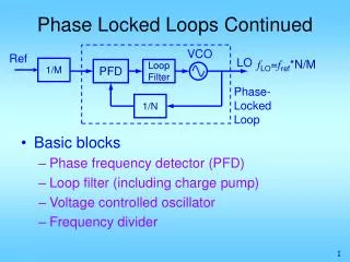
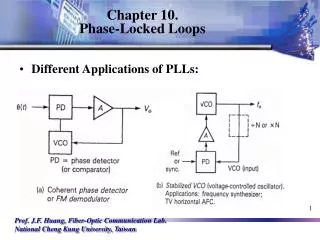
Phase-Locked Loop • Phase Detector (PD): This is a nonlinear device whose output contains the phase difference between the two oscillating input signals. • Voltage Controlled Oscillator (VCO): This is another nonlinear device which produces an oscillation whose frequency is controlled by a lower frequency input voltage. • Loop Filter (LF or LPF): While this can be omitted, it is always conceptually there since PLLs depend on some sort of low pass filtering in order to function properly • A feedback interconnection: Namely the phase detector takes as its input the reference signal and the output of the VCO. The output of the PD, the phase error, is used as the control voltage for the VCO.
PLL Architectures – Linear PLL vs Digital PLL • No frequency tracking • Input amplitude dependency • Nonlinear phase detector gain • No frequency tracking • Duty-cycle sensitivity (can be solved by edge triggered phase detector
PLL Architectures – All-digital PLL • Lower sensitivity to digital-switching noise • Easier to transfer a design between technologies • Faster lock-in times • Higher complexity • Bigger die size • No true frequency synthesis (in general)
PLL Architectures - Charge Pump PLL • Stability: Two poles at the origin • Zero in LPF • Auxiliary charge pump • Zero phase error (ideally) • Unlimited capture range (ideally)
Oscillation Control in Charge Pump PLLs • Charge Pump PLL: contemporary applications • PFD and charge pump nonidealitites: 45% of the output phase jitter1 • Phase-Frequency Detector • Possible dead zone • Possible duty-cycle dependency • Possible unbalanced output generation • Charge Pump • Possible current asymmetry • Possible current leakage • Clock skew in Clock/Data Recovery • Reference spur in Frequency Synthesis 1V. Kaenel, D. Aebicher, C. Piguet, and E. Dijkstra, “A 320 MHz 1.5mW @ 1.35 V CMOS PLL for microprocessor clock generation,” in Journal of Solid-State Circuits, Vol. 31, No.11, Nov. 1996.
Phase-Frequency Detector - Behavior • Three-state device • PLL capture range • Maximum operating frequency: orthogonal inputs • Reset pulse • Too short = dead zone • Too wide = VCO control perturbation
Charge Pump - Behavior • Iup: charging current • Idn: discharging current • S1, S2: switches Effective charge pump requirements: • Equal charge/discharge current at any CP output voltage • Minimal charge-injection and feed-through (due to switching) at the output node • Minimal charge sharing between the output node and any floating node, i.e. MOS switches at off position
Single-ended control for multi-GHz • charge-pump PLLs • Design of a low-noise 1.8 GHz charge-pump PLL
Phase-Frequency Detector - Design • 0.18μ TSMC CMOS • Differential outputs • Reset pulse = 0.2ns VDD=1.8V • Maximum frequency ≈ 600 MHz • Significant power dissipation above 100 MHz
Single-Ended Charge Pump – Design Replica Biasing • No charge sharing • No charge injection
Differential VCO with Single-Ended Control Saturated Gain Stage with Regenerative Elements • Delay control by varying latch strength • Two sets of inputs for multiple-pass architecture • Tuning range control by varying M3 and M4 sizing Delay Stage : C.H. Park, and B. Kim, “A Low-Noise, 900-MHz VCO in 0.6-m CMOS,” IEEE J. Solid State Circuits, vol. 34, pp. 586-591, May 1999.
Differential VCO with Single-Ended Control 9-Stage Multiple-Pass Loop • Auxiliary loops nested inside main loop • Frequency Improvement • Effective stage delay reduced • Noise Improvement • Slew rate increased
Differential VCO with Single-Ended Control Testing Issues • Current-mode logic dividers: 1/2 to 1/64 of actual frequency • Current-mode logic buffers • DTOS: Differential to single-ended conversion • Driver chain • Turn-off circuitry to reduce cross-talk
Differential VCO with Single-Ended Control Simulation vs Measurement • VCO Range • Simulation: 1.16 – 1.93 GHz • Measurement: 1.10 – 1.86 GHz
1.8 GHz Low-Noise PLL Measurement Summary • Off-chip LPF: flexibility in testing
Single-ended control for multi-GHz • charge-pump PLLs • Design of a low-noise charge-pump PLL for maximum frequency
Differential VCO with Single-Ended Control 3-Stage Multiple-Pass Loop • VCO Range • Simulation: 5.18 – 6.11 GHz • Measurement: 5.35 – 6.11 GHz
Differential VCO with Single-Ended Control Phase Noise for the 3-Stage Multiple-Pass Loop Measurement Simulation: SpectreRF Power Spectrum at ¼ Output of the 3-Stage Ring Power Spectrum at 5.79 GHz center frequency • Simulation: -99.5 dBc/Hz @ 1 MHz offset from ~6 GHz central frequency • Measurement: -99.4 dBc/Hz @ 1 MHz offset from ~6 GHz central frequency
Differential control for multi-GHz charge-pump PLLs
Differential Charge Pump – Design • Output linear range (0.315V, 1.390V) • Differential outputs: FST and SLW
Charge Pump – Common-Mode Feedback (CMFB) • Sampled data CMFB • CMFB transconductance gain: 40µA/V • CMFB bandwidth: 3KHz • CMFB phase-margin: 76º • Capacitors • DC voltage stability • Diodes • No effect on operation • Discharging metal during the etching process 100µA
Charge Pump - Layout 150 x 130 µm2
Charge Pump – Post Layout Simulation • High output resistance • No charge sharing • Decreased charge injection
Differentially Controlled LC Oscillator - I Accumulation mode MOS varactor • Differential fine tuning: Accumulation mode MOS varactors • Digital coarse tuning: MiM capacitors • Three-turn inductor • 2.4 nH, 1.7mm, Q~9.5 • Thick top metal • Frequency goal: 2.5GHz
Differentially Controlled LC Oscillator - II 1/16 output fo = 157.8 MHz PN@100KHz = -83.8 dBc/Hz
PLL – Test Setup • Stable nested loops • CMFB BW ≈3KHz<<Loop BW ≈200KHz<<Reference ≈150 MHz
PLL - Measurement • Phase lock @ 2.5 GHz internal frequency • Phase Noise @ 1MHz offset from 2.5 GHz: as low as –123 dBc/Hz Reference ½ Output
Prototype Chip in 0.18μm TSMC CMOS • Analog Layout Techniques • Common centroid topology • Stacked parts with dummy components • Guard rings • Routing • Matched and short busses • Decoupled parallel analog and digital lines • Complimentary digital signals crossing analog buses • Power • Analog and digital supplies merging as close to the pad as possible • Wide supply busses at the top metal • Pads • Electrostatic discharge protection within the custom designed analog I/O pads
Single-Ended vs Differential Control • For a given frequency range Vdd KVCO • Increased KVCO causes a higher sensitivity to the control line perturbation • For Vctrl = Vmcosωmt • Differential Control Line • Doubles Dynamic Range to drop the spur level by 50% • Common mode rejection lowers the spur levels
PLL Performance Comparison - I Maximum frequencies of published PLLs Phase noise versus maximum frequency
PLL Performance Comparison - II Reported output jitter vs measured jitter Reported normalized jitter vs measured jitter
Clean vs Noisy Supply Voltage • Increase in jitter • Single-ended: 20-35 times • Differential: 6 times Periodic cycle-to-cycle jitter in noisy environment: significance of the control line noise
PLL Phase Noise Improvement - I • ↑ Temperature → ↑ Leakage ≡ Loss of lock at low frequencies • Solution: Multiple reset pulses in lock: up’, dn’ • Solution: Adaptive multiple pulses in lock: up’’, dn’’
PLL Phase Noise Improvement - II Static Phase Error Improvement • Best case phase skew for • ICP = 70 µA • ILEAKAGE = 0.01 ICP • ICP modulation by CMFB: up to 30µA
PLL Phase Noise Improvement - III • M = 8 • ~6dB improved output spur level • M = 32 • ~20dB improved output spur level
Oscillation Control Summary in Charge Pump PLL • Periodical disturbance of the VCO control line • Process, voltage, and temperature (PVT) variations of the LPF components • Large area consumption by LPF components • Limited acquisition time • Analog control drawbacks determined by CMOS trends • Reduced linear range (decreasing supply voltage) • Significant leakage and weak-inversion currents (decreasing feature size) • Power supply and substrate noise (increasing integrity)
Digital Control and Analog Oscillator • Immune to current leakage • Immune to supply/substrate noise • Tolerant to process variations • Semi-custom loop design • Monitoring of the internal loop states • Quantization noise introduced by the DAC Precision in oscillation control
REF VCO DN UP VCO Leads In Phase VCO Lags REF VCO DIR MOD VCO Leads In Phase VCO Lags Pulse-Stream Coded Phase-Locked Loop A novel method to render digital control: Phase/frequency comparison coded by pulse trains Dual Pulse-Stream PFD: Single Pulse-Stream PFD:
A Simplified Pulse-Stream Coded PLL Prototype Single Pulse-Stream PFD: • 0.18μ TSMC CMOS • Highly parameterized for testing basic characteristics • 3-stage current-controlled oscillator • Active load differential pair stages • 4-bit shift register
A Simplified Pulse-Stream Coded PLL Prototype Control Signals: • Control 1: pulse width (1-1.6ns) • Control 2,3: delay (0.2-1.5ns) • Control 4: DAC step current • Control 5: CCO bias (100-200 MHz)