Delay Locked Loops and Phase Locked Loops
310 likes | 554 Vues
Delay Locked Loops and Phase Locked Loops. Motivation: System. U1. U2. G1. FF2. FF1. B2. B4. B1. B3. CLK. Analysis Setup Time Calculation. The setup time at FF2 is calculated from the common point CLK. Use the maximum delay to set up FF2:D (G1 output)

Delay Locked Loops and Phase Locked Loops
E N D
Presentation Transcript
Motivation: System U1 U2 G1 FF2 FF1 B2 B4 B1 B3 CLK
AnalysisSetup Time Calculation The setup time at FF2 is calculated from the common point CLK. Use the maximum delay to set up FF2:D (G1 output) Use the minimum delay to drive FF2:CLK (B4 output) To drive the data we add (max) B1 B2 FF1 (CLK -> Q) G1 FF2 (tsu) If the CLK at FF1 would occur at exactly the same time as CLK on the board, then the delays for B1 and B2 would effectively be zero. Note that this technique relies on the max delays being eliminated being greater then losing the minimum delays in the clock path.
Setup Time Flow U1 U2 Use max for data path G1 FF2 FF1 B2 B4 B1 B3 CLK Use min for clock path
AnalysisHold Time Calculation The hold time at FF2 is calculated from the common point CLK. Use the minimum delay to set up FF2:D (G1 output) Use the maximum delay to drive FF2:CLK (B4 output) To drive the clock we add (max) B3 B4 FF2 (th) If the CLK at FF2 would occur at exactly the same time as CLK on the board, then the delays for B3 and B4 would effectively be zero. Since the delay through U1 and U2/G1 can not be zero, then if FF2:th = 0, we can design the system as if flip-flops in U2 have a zero hold time at the device’s input pins. That is typically how we designed with “good” SSI and MSI devices.
Hold Time Flow U1 U2 Use min for data path G1 FF2 FF1 B2 B4 B1 B3 CLK Use max for clock path
Motivation: Clock Control • Locking to external signals • Phase control • Frequency Multiplication • Frequency Division
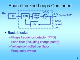
Basic Phase Locked Loop LowPass Filter Phase Detector Voltage Controlled Osc. Analog Circuit
Example: PLL Multiplication LowPass Filter Voltage Controlled Osc. Phase Detector Divide by n
Example: PLL Multiplication LowPass Filter Voltage Controlled Osc. Phase Detector Divide by n Single Event Upset Heavy Ion or Proton
DLL Another TechniqueGoal: System Clock Matches Clock at F-F U1 FF1 CLK Ideal 0 ns
Buffer Tree Delays Not Negligible CLK FF1:CLK
Buffer Tree Delays Not Negligible So Add A Delay CLK FF1:CLK Delayed CLK
Buffer Tree Delays Not Negligible Add A Bit More Delay CLK FF1:CLK Delayed CLK More Delay
Buffer Tree Delays Not Negligible Add Just A Bit More Delay CLK FF1:CLK Delayed CLK More Delay A Bit More
What Did We Do? CLK FF1:CLK Delayed CLK More Delay A Bit More
DLL Another TechniqueInsert “Proper” Delay U1 FF1 CLK Goal: Insert Delay to Make The Difference Zero If We Delay Things “Enough” To Line Up Corresponding Edges of Different Cycles.
DLL Principle Of Operation Delay Line
DLL Principle Of Operation Delay Line Single Event Upset Heavy Ion or Proton
Manufacturers’ Selections • Actel • AX: PLL • ProAsic, ProAsic+ ??????? • Xilinx Virtex: DLL • Chip Express • QYH500: DLL • CX2000: PLL • CX3000: PLL
Virtex Architecture Overview IOB = I/O Block DLL = Delay-locked loop BRAM = Block RAM (4,096 bits ea.) CLB = Configurable Logic Block
Virtex DLL • Uses discrete digital delay line • Latency: 1 to 4 clock periods • 4 Quadrature phases • Can double frequency • quadruple if two DLL’s used • Divide by 1.5, 2, 2.5, 3,4,5,8, or 16 • Deskew board clock • Multiple FPGAs, other devices
Board Level Clock De-Skewing Note: Can include multiple Virtex devices.
Chip Express QYH500 DLL Single Event Upset Heavy Ion or Proton
AX PLL • Fout = Fin * i / j • 1 i,j 64 • Programmable delays • 250 ps steps, Range ± 3.75 ns • Can cascade up to 8 PLLs
+1.5V AX PLL: External Components Board FPGA
Key Parameters • Minimum and Maximum Frequencies • Tolerance on input signals • Frequency • Jitter • Lock Time • Output Phase Offset • Output Jitter
Timing Analysis CLK With a crystal clock oscillator, the time from rising edge to rising edge (or falling edge to falling edge) is quite stable, with crystal clock oscillators having relatively low jitter and good short term stability.
CLK Timing Analysis Max • With DLL and PLL, one must check the jitter specifications carefully, to assure that worst-case timing must be met. • Analysis must include the time before the loop locks. • Analysis must include the effects of SEU’s on the loop’s control circuits. Min