Dedicated Peripheral Interface Device (Introduction to 8255)
Dedicated Peripheral Interface Device (Introduction to 8255). Dr A Sahu Dept of Computer Science & Engineering IIT Guwahati. Hierarchy of I/O Control Devices. 2 Port (A,B), No Bidirectional HS mode (C) 4 mode timer. 8155 I/O + Timer. 8255 I/O. 2 Port (A,B) A is Bidirectional

Dedicated Peripheral Interface Device (Introduction to 8255)
E N D
Presentation Transcript
Dedicated Peripheral Interface Device (Introduction to 8255) Dr A Sahu Dept of Computer Science & Engineering IIT Guwahati
Hierarchy of I/O Control Devices 2 Port (A,B), No Bidirectional HS mode (C) 4 mode timer 8155 I/O + Timer 8255 I/O 2 Port (A,B) A is Bidirectional HS mode (C) Extra controls 8253/54 Timer 6 mode timer 8259 Interrupt controller 8237 DMA controller 8251 Serial I/O USART controller
Outline • 8155 I/O Interface & Timer • Dedicated I/O interface (8255) • Dedicated Timer (8254/8253) • 8255 Ports and mode of operations • Interfacing A/D Converter using Handshake mode using 8255
8155 Features • IO Capability: • 2kbits static RAM 256x8 • 2 programmable 8 bit I/O ports • 1 programmable 6 bit I/O port • Timer Capability: • 1 programmable 14 bit binary counter/timer • 4 Modes Reset in RD WR Port A Mode 00 RAM N/2 N/2 CE PA0-PA7 Mode 01 N/2 N/2 N/2 N/2 IO/M Port B Mode 10 AD0-AD7 N PB0-PB7 Mode 11 ALE N N Port C PC0-PC5 Timer CLK Timer MSB LSB Timer Out
Expanded Block Diagram CEb CWR Latch Port A AD0-AD7 A0-A7 PA0-PA7 3 to 8 Decoder Port B 0 1 2 3 4 5 ALE A2 PB0-PB7 D7-D0 A1 Port C A0 PC0-PC5 Timer MSB LSB Timer Out Clock for timer
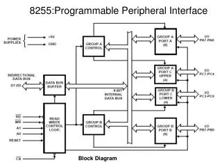
Block Diagram of 8255 Gr A Port A (8) I/O PA7-PA0 Group A Control I/O PC7-PC4 Gr A Port C (H 4) Bi directional Data Bus D7-D0 Data Bus Buffer Gr B Port C (L 4) I/O PC3-PC0 8 bit Internal Data Bus Read Write Control Logic RDb WRb A1 A0 RESET CSb Group B Control Gr B Port B (8) I/O PB7-PB0
Ports & Modes in 8255 8255 Port A D7 D6 D5 D4 D3 D2 D1 D CU Port C 0/1 CL Port B BSR Mode Bit Set/Reset I/O Mode BSR Mode Bit Set/Reset For Port C No Effect on I/O Mode Mode 0 Simple I/O for Ports A, B & C Mode 1 HS mode for Ports A and/or B Port C bits are used for HS Mode 2 Bidirectional Data mode for Port A B can in mode 0/1 Port C bits are used for HS
7 6 5 4 3 2 1 0 D7 D6 D5 D4 D3 D2 D1 D0 Group B Port C(L) – 1 Input 0 output Port B – 1 Input 0 output Mode select: 0 mode 0; 1 mode 1 Port C(U) – 1 Input 0 output Port A – 1 Input 0 output Mode select: 00 mode 0; 01 mode 1; 0x mode 2 1 – mode select 0 – bit set/reset Group A Ports & Modes in 8255 : Control register
I/O port Addressing 8255 A7 A6 A5 A4 A3 A2 Port A=80H CSb A1 A0 RDb WRb Port C=82H A1 A0 IORb IOWb Port B=81H Reset Reset
BSR (Bit Set or Reset Mode) • Set/Reset bit of Port C • Heavily used for HS and Interrupt mode • BSR Control word • BSR Control word • To set PC7= 0 000 111 1 (0FH) • To reset PC7= 0 000 111 0 (0EH) • To set PC3 = 0 000 011 1 (07H)
Group A Group B Port A Upper C Lower C Port B Ports • Control register controls the overall operation of 8255 • All three ports A, B and C are grouped into two
Operation modes • 8255 has three modes: - mode 0: basic input-output - mode 1: strobed input-output - mode 2: strobedbidirectinal bus I/O • In mode 0 - two 8-bit ports and two 4-bit ports - any port can be input or output - Outputs are latched, inputs are not latched
Mode 0 Port A Upper C Lower C Port B
Operation mode 1 • In mode 1: -three ports are divided into two groups -each group contains one 8-bit port and one 4-bit control/data port - 8-bit port can be either input or output and both latched - 4-bit port used for control and status of 8-bit data port
Group A Group B Port A Upper C Lower C Port B Mode 1
Operation mode 2 • In mode 2 - only port A is used - port A becomes an 8-bit bidiectional bus - port C acts as control port (only pins PC3-PC7 are used)
Mode 2 Group B Group A Port A C7-C3 Port B
PA[7:0] PC7 OBFA PC6 ACKA PC4 STBA PC5 IBFA 8255 PC3 INTRA PC0 In Out In Out In Out STBB OBFB IBFB ACKB INTRB INTRB PC0 PC0 PB[7:0] Mode 1 Mode 0 Programming 8255 • Mode 2: • Port A is programmed to be bi-directional • Port C is for handshaking • Port B can be either input or output in mode 0 or mode 1
Reference • R S Gaonkar, “Microprocessor Architecture”, Chapter 15