Download
1 / 24
420 likes | 1.16k Vues
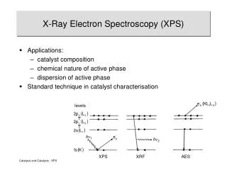
Introduction to Auger Electron Spectroscopy (AES). Center for Microanalysis of Materials Frederick Seitz Materials Research Laboratory University of Illinois at Urbana-Champaign. What is Auger?.

E N D
Introduction to Auger Electron Spectroscopy (AES) Center for Microanalysis of Materials Frederick Seitz Materials Research Laboratory University of Illinois at Urbana-Champaign
What is Auger? Auger Electron Spectroscopy (AES) is a widely used technique to investigate the chemical composition of surfaces.
Why the Odd Name? Pierre Victor Auger (May 14, 1899 – December 24, 1993) was a French physicist, born in Paris. He worked in the fields of atomic physics, nuclear physics, and cosmic ray physics.[1] The process where Auger electrons are emitted from atoms is used in Auger electron spectroscopy to study the elements on the surface of materials.[1] This method was named after him, despite the fact that Lise Meitner discovered the process a few years before in 1922. http://en.wikipedia.org/wiki/Pierre_Victor_Auger
STEP 3 KLL Auger electron emitted to conserve energy released in step 2 STEP 1 Ejected electron FREE ELECTRON LEVEL CONDUCTION BAND FERMI LEVEL Auger Transition Named: KLL VALENCE BAND STEP 3 (alternative) an x-ray is emitted to conserve energy released in step 2 E(Auger)=E(K)-E(L2)-E(L3) E(X-ray)=E(K)-E(L2) L3 2p L2 2s L1 STEP 2 L electron falls to fill vacancy Incident Electron 1s K
Auger Energy Scale • The AES instrument measures the kinetic energy of all collected electrons.
Auger Stats • Primary Beam = 3 - 20 KeV electrons • Detection Sensitivity = ~1 atomic % • Sampling Distance (depth) = 2 to 4 nm • Analysis Diameter = 80nm to several mm • Elements Detectable = Li and above
Auger Data Formats Raw Data Differentiated Data
Peak Height / Quantitation For quantitation the derivative form of the data is used. Sensitivity Factors are used to adjust the peak heights of all elements present in the sample. The composition is normalized to 100% to determine the amount of each element.
Additional Capabilities of Auger Spectroscopy • Identify surface contaminants and composition. • Study composition as a function of depth. • Analyze sample features as small as 80nm. Using an electron gun for the primary beam allows small analysis spot sizes.
Why UHV for Surface Analysis? Pressure Torr Degree of Vacuum • Remove adsorbed gases from the sample. • Eliminate adsorption of contaminants on the sample. • Prevent arcing and high voltage breakdown. • Increase the mean free path for electrons, ions and photons. 2 10 Low Vacuum -1 10 Medium Vacuum -4 10 High Vacuum -8 10 Ultra-High Vacuum -11 10
AES Instrument Configuration • Elements of Typical Auger System: • Electron Gun • Analyzer • Secondary Electron Detector • Ion Gun • Sample Stage • Introduction System
Significance of Primary Beam The Electron Beam is functioning both as the imaging beam and the primary beam for analysis. This means that the area of interest on the sample can be directly aligned for analysis.
MRL Instrumentation PHI Model 660 Scanning Auger Microprobe
Al/Pd/GaN Thin Film Example (cross section)
Permissions • Used with explicit permission from Center for Microanalysis of Materials • I have reformatted some of the pages • Please do not duplicate / redistribute