Electron spectroscopy
Electron spectroscopy. IMFP of electron Photoelectron spectroscopy 3. Microscopies: PEEM, LEEM, Imaging XPS Auger electron spectroscopy Extended X-ray Absorption Fine Structure. References: 1. Electron spectroscopy, theory, techniques, and applications I-IV,

Electron spectroscopy
E N D
Presentation Transcript
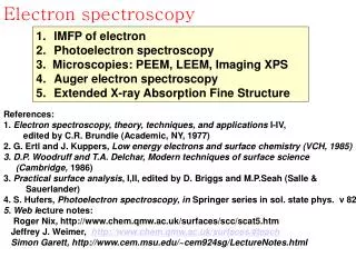
Electron spectroscopy • IMFP of electron • Photoelectron spectroscopy • 3. Microscopies: PEEM, LEEM, Imaging XPS • Auger electron spectroscopy • Extended X-ray Absorption Fine Structure References: 1. Electron spectroscopy, theory, techniques, and applications I-IV, edited by C.R. Brundle (Academic, NY, 1977) 2. G. Ertl and J. Kuppers, Low energy electrons and surface chemistry (VCH, 1985) 3. D.P. Woodruff and T.A. Delchar, Modern techniques of surface science (Cambridge, 1986) 3. Practical surface analysis, I,II, edited by D. Briggs and M.P.Seah (Salle & Sauerlander) 4. S. Hufers, Photoelectron spectroscopy, in Springer series in sol. state phys. v 82 5. Web lecture notes: Roger Nix, http://www.chem.qmw.ac.uk/surfaces/scc/scat5.htm Jeffrey J. Weimer, http://www.chem.qmw.ac.uk/surfaces/#teach Simon Garett, http://www.cem.msu.edu/~cem924sg/LectureNotes.html
Electron Spectroscopies • Auger Electron Spectroscopy (AES) • X-ray Photoelectron Spectroscopy (ESCA) • Ultraviolet Photoelectron Spectroscopy (UPS) • Electron Energy Loss Spectroscopy (EELS) • High Resolution EELS • Electron Microscopies • Scanning Auger Microscopy (SAM) • Photoemission Electron Microscopy (PEEM) • Low Energy Electron Microscopy (LEEM) • Scanning X-ray Photoelectron Microscopy • (SXPEM) • Secondary Electron Microscopy with • Polarization Analysis (SEMPA) Acronyms
Why are electron spectroscopies surface sensitive ? 100 IMFP(nm) 10 1 0 • 10 100 1000 10000 • Energy (eV) The inelastic mean free path (IMFP) of electrons is less than 1 nm for electron energies with 10~1000 eV.
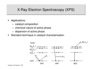
Photoelectron Spectroscopy X-ray Photoelectron Spectroscopy (XPS) :hv=200~2000 eV or Electron Spectroscopy for Chemical Analysis (ESCA) Ultraviolet Photoelectron Spectroscopy (UPS): hv =10~50 eV e photoelectron KE KE: kinetic energy BE: binding energy F: work function hn(E,p,q) e(E,q,s) Ev f Ef hn BE KE = hv – BE – f for soild KE = hv – BE(or IP) for gas
PES spectra KE EF Valence electrons Core electrons hn Secondary electrons Evac EF Valence band Core level
Typical XPS spectra KE KE • steplike background due to inelastic electron energy loss • Electrons from deep bulk(depth>IMFP) loose their KE energies (higher BE)
Photoemission peak intensity I(E, hv) ~ Nv(E) Nc(E) s(E,hv): UPS limit ~ Nv(E)s(E,hv): XPS limit, where Nv(E): densities of initial states(i) Nc(E): densities of final states(f) s(E,hv): photoionization cross section s~ |<f|AP|i>|2 The XPS spectra represent the total density-of-states modulated by the cross-section for photoemission
Transition dipole moment Hamiltonian under electric field H = (1/2m)(p-eA/c)2 + V(r) Ho= p2/2m + V(r) H’= -eA.p/mc Mif =<f|H’|i>=(e/mc)<f|Ap|i> = (e/mc)<f| Aoexp(ikx).p|i> let unit vectore=Ao/|Ao|: the direction of polarization = (e/mc)<f| e.p|i> Vector potential A(x,t) = Aoexp(ikx-vt): electromagnetic wave exp(ikx) = 1 +ikx - (kx)2~1: dipole approximation kx=2p/5000Ǻx1Ǻ ~10-3 for the visible light of l=500nm k: photon wave vector Electron momentum operator p = -i <f||i> = (i/ℏ) <f|p|i> = (mv/ℏ)<f|r|i> = (mv/eℏ)<f|er|i> = (mv/eℏ) <f|m|i> m:electric dipole moment = (1/ℏv)(<f|V|i>
Koopman’s Theorem: frozen orbital approximation A(N) + hv A+(N-1) + e e hv + e(KE) initial state final state Ei(N) + hv = Ef(N-1) + KE BE = hv –KE = Ef(N-1) - Ei(N) = -eiHF - erelax+ ecorrel BE of core level≈ - eiHF( ith orbital energy)
Chemical Shift of Binding Energy Valence shell Electron charge q r Core electron e The core electron feels an alteration in the chemical environment when a change in the charge of the valence shell occurs. A change in q, dq, gives a potential change dE = e dq/r • the oxidation state of the atom • the chemical environment • - electronegtivity of neighboring atoms • - # of neighboring atoms
Binding energies in solids BE = BE(atom) + e2q/rv + UM eq: charge transferred to the ion rv: radius of valencesehll UM: Madelung energy (ae2q/ d) rv rv d Chemical shift in compound A and B DBE(A,B) = e2(qA-qB)/rv + UM(A)- UM(B) Ist term: the difference in the Coulomb interaction between the core and valence electrons 2nd term: interaction of the atom to be photoionized with the rest of the crystal
Core level spectra of silicon oxides F.J. Himpsel et al., Phys. Rev. B 38, 6084 (1988). J.W. Kim et al (2001)
Example of Chemical Shift • The chemical shift: ~4.6 eV • Metals: an asymmetric line shape (Doniach-Sunjic) • Insulating oxides: more symmetric peak
Spin-orbit Coupling J = L+S J = L-S Pd: (3d)10+ hv(3d)9+ e L =2 , S = ½, J = L+S,…, L-S = 5/2, 3/2 2D 5/2 g J = 2x{5/2}+1 = 6 2D 3/2 g J = 2x{3/2}+1 = 4 • p,d and f orbitals splitted into two peaks in XPS spectra • BE (J=L-S) >BE(J=L+S) • Splitting as Z , n
Photoemission features • XPS peaks: Main peak and extra satellite peaks • Source of satellite peaks • Intrinsic part : created in the photoemission process • Extrinsic part : interaction of photoelecton with the other • electrons in the solid • Initial state effects • Final state effects • Sample charging effects • Nonmonochromic photon source Ref: Electron spectroscopy I-IV edited by C.R. Brundle and A.D. baker Photoelectron spectroscopy by S. Hufner
Extra peaks: final state effect • Initial state effect: Koopman’s theorem • Final state effect: : 1~10 eV • the created core hole after photoionzation affects the energy • distribution of the emitted electrons in different ways. • Relaxation effects • Multiplet splliting • Multielctron excitations • shake up and shake off satellites • electron-hole excitation (continuous satellite): asymmetric line shape • Plasmon loss peaks • Vibrational effects
Relaxation effect Localized core hole created by photoionization is delocalized by The movement of electrons from the photoexcited atom or neighboring atoms, causing the photolectrons with lower BE than the adiabatic BE BE = BE(Koopman)-erelax erelax = erelax(intra) + erelax(extra) Intra-atomic relaxation - redistribution of the electron of the excited atom - free atom case Extra-atomic relaxation - redistribution of electrons from neighboring atoms - molecules, solids cases -BE of the solid phase element is lower 5~10eV than BE of the corresponding gas phase element
Multiplet Splitting • due to the various possible non-degenerate total electronic states that • can occur in the final states Fe 3+(3s23d5) + hv Fe 4+(3s13d5) + e 3d 3s Initial state Final state Terms: 6S 7S 5S
Shake up and shake off Sudden approximation -In experiment, one cannot observe adiabatic energy since atom does not have time to relax to ground ionic state -photolectron is ejected while the atom is in the excited state • Multi-electronic transitions after creation of Ne 1s core hole • - Excitation of electron to higher bound state: shake up • - Excitation to continuum state: shake off Excited state Ground state hv A
Satellite peaks Initial state 3d9L Final state: Main peak: c-1d10L-1 Satellite peak: c-1d9L
Multielectron excitations in metals: Doniach-Sunjic line shape -asymmetric line shape due to the electron-hole excitation near Fermi level -proprotinal to the density-of-state at Fermi level
Energy loss features • interaction between photoelectron and other electrons • in the surface region • -interband electronic transition • -plasmon energy loss e hn KE plasmon: a quantum of a plasma oscillation vp= 4pne2/m Bulk plasmon (ħvp) = 15.8 eV surface plasmon (2ħvp)
Sample charging effect • insulating sample will be charged positively due to the loss • of the electrons in solids by photoionization e e KE hn KE + + + + + + + + + + Positively charged sample Neutral sample • shift to lower KE, thus 1~5 eV higher BE • How to prevent charging ? • use flood electron gun to compensate charging • use thin film sample on the metallic substrate
K. Shabtai, I.Rubinstein,* S. R. Cohen, and H. Cohen* J. Am. Chem. Soc., 122 (20), 4959 -4962, 2000. Differential charging Flood Gun off Monolayer Self-Assembly. The surface was pretreated by UV-ozone + ethanol dip.Decanethiol (DT) was adsorbed (2 h, 4 mM solution in bicyclohexyl), the sample was rinsed with chloroform followed by octadecane trichlorosilane (OTS) adsorption (2 min, 2 mM solution in bicyclohexyl) and rinsing with chloroform Flood Gun on
Photon source • X-ray source • Mg/Al anode source • - beam sieze: 1cm • flux: 1010~1012 • Rotating anode source • Ulraviolet light source • He discharge source • He(1P1) He(1S0) + hv(21.2ev) • flux: 1010~1012 • Line width ~ a few meV
hn= 2.2x10³E3(GeV)/R(m) Synchrotron radiation • Tunable: wide photon energies (IR to hard X-ray) • High intensity: 1012~1015 photons/sec • high brightness • Polarization • Pulsed beam
http://pal.postech.ac.kr/english.html Pohang Light Source (PLS) Beam energy 2~2.5 GeV Beam pulse Length ~1 ns Buch length 17~20 ps Beam current ~1 A
Electron source J.J. Weimer, MTS273, UAH
Energy analyzer • Hemispherical analyzer • Cylnidrical mirror analyzer • Cylindrical defelction analyzer • Paraboloidal analyzer • Display type analyzer • Time of flight analyzer From J. J. Weimer, UAH • Hemispherical anlayzer • E = e(V2-V1)/(R2/R1- R1/R2) • DE/E = (w1+w2)/Ro + (da)2 • ~ 10-3 ~10-4 • w1,w2: width of input and output slits • R1,R2: radius of inner and outer spheres • da : spread of entrance angle a • angle resolved a = 10~20o • multichannel detector to enhance • counts • -High energy and angle resolution
Energy analyzer (continued) • Cylindrical morror analyzer • E = 1.3099eVln(R2/R1) • DE/E = 0.18w/R1 + 1.375(da)3 • ~ 10-2 ~10-3 • R1,R2: readius of inner and outer • cylinder • w : annular slit width • da : Spread of entrance angle a • High transmission • Sensitive to sample position w
Detector • Electron multiplier • Channeltron • single channle detection • Multichannel plate • - multichannel detection • - 2D-imaging Typical gain : 103~106 bias voltage: 1-5kV 1e = 1.6 x10⁻¹⁹ C 1.6 x10-19x106 = 1.6x10-13 = 0.16 pA
Quantitative analysis Intensity = peak area after back ground subtraction ~ # of atoms in the detected volume The intensity of a core level of an element A IA = sAD(EA)LA(gA)JoNA T(EA) lM(EA) cosq sA: photoionization cross section D(EA) : Detection efficiency of the electron spectrometer LA(gA) : The angular asymmetry of the emitted w.r.t. the angle between the direction of incidence and of detection LA(gA) = 1 + (1/2)bA((3/2)sin2g-1) Jo: The flux of photon T(EA) : The transmission of the analyzer NA: The density of atoms A lM : Inelastic mean free path of electron Concentration of A CA CA = IA/SA IA = measured intensity SA= sensitivity factor of A • Accuracy • use SA<15% • use standards< 5% • Precision <2%
Background subtraction • straight line • Shirely’s method • Tougard and Sigmund: • Phys. Rev. B 25, 4452 (1982) • Caution: • -change in peak position, width, height Primary excitation spectrum F(E) = J(E) -liK(E’-E)J(E’)dE’ liK(E’-E) = B(E’-E)/[C+(E’-E)2]2 B=2866 eV, C = 1643 eV for Cu, Ag, Au J(E): measured flux of emitted electrons at E li: the mean free path of electron K(E’-E): the probability that an electron of E shall lose energy E’-E per unit path length travelled in the solid
Applications • Determination of energy levels • Chemical bonding • Oxidation states • Density-of-states of valence bands • Energy bands • Quantum well states • Quantitative analysis
Angle-Dependent Analysis Silicon Wafer with a Native Oxide X= dcosq x q d Si 2p peak of the oxide (BE~103eV) increases at grazing emission angles
Example: CdSe-Nanoparticles TOPO: n-trioctylphosphine oxide Se 3d • Unstable to photoxidation • Chalcogenide at the surface • is oxidized to sulfate or selenate • and evaporate as molecular • species
Example:polymer The number of CH2 groups Ns= (2-15RO/C)/RO/C at the BA surface RO/C: O to C atomic ratio Ns= (6-15RF/C)/RF/C at the FBA surface RF/C: F to C atomic ratio L. Li et al, Macromolecules 33, 8002(2000)
Example: SAM/AU M-C Bourg et al, J. Phys. Chem. B 104, 6562 (2000)
Example:Biomolecules/SAM/Au C-M Yam et al, Coll. Surf. B21, 317 (2001)
Imaging XPS Si SiOx • Scan Analyzer • Parallel Direct Imaging • X-ray microprobe/Zone plate Present: Submicron resolution
Low Energy Electron Microscopies Step decoration of Si(111) • Strong elastic backward scattering of slow electrons • (10~100eV) • Several monolayer sensitivity • Resolution: ~ 20 nm LEEM: E Bauer, Rep. Prog. Phys. 57, 895 (1994)
Photoelectron Emission Microscopy Array detector Cathode Lens hv e Ground Resolution : 20~100nm A threshold excitation lamp. g-Arc lamp, operating at 4.9 eV Due to the presence of oxide at the silicon surface,Si appears DARK (W >> 4.9 eV) and Pd appears BRIGHT (W = 5.12 eV ~ 4.9 eV)
Scanning Transmission X-ray Microscopy X-ray microscope image, and protein and DNA map, of air-dried bull sperm. Images were taken at six x-ray absorption resonance wavelengths, and were used to derive the quantitative maps. Zhang et al., J. Struct. Biol. 116, 335 (1996). hv =10-1000 eV l = 0.1-10 nm
Auger Electron Spectroscopy Auger electron e 2p3/2,1/2 L2,3 L1 K 2s hv or e e 1s KE = EK– EL1– EL23 Kinetic Energy of Auger Electrons for KLL Transition Element Specific