Modulation Formats
Modulation Formats. Modulation Formats. General. Optical communication systems are carrier systems . This implies that a wave of a frequency much higher than that of the information ( signal) is used to enable the


Modulation Formats
E N D
Presentation Transcript
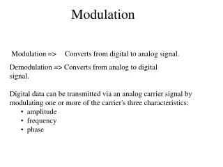
Modulation Formats General • Optical communication systems are carrier systems. This implies that a wave of a • frequency much higher than that of the information ( signal) is used to enable the • information to be transported through the channel. The range of wavelength over • which optical communications operate ranging from , say, 1 to 2 μm. This wavelength • range corresponds to a frequency range 1.5x10² to 3x10² THertz. Remember, • 1 THerz=1x10¹² Hertz. The bandwidth of the information sources currently available to • us is far away from this number. The carrier features should be suitable to propagate • in the channel under consideration and the next question is how does a information • carrying signal is “loaded” on a carrier to go through the channel? • The process that achieves this objective is called “modulation” and has been a subject • of intensive study since the inception of electronic communications back in the 1920s. Modulation is the process of conveying an information signal inside another signal (carrier) that can be physically transmitted. This is achieved by varying one or more of the properties of the signal that can be transmitted.
Modulation Formats General • There is two classes of modulation processes; analogue and digital. • Analogue modulation; a signal is defined as analogue if it is continuous in both • time and any other parameter that characterised it. Then, if that signal is applied continuously on the carrier the outcome is an analogue modulated signal. Mathematically, the concept is defined through the definition of the continuous function. A function f (x) is continuous at x = a if • Digital modulation; a signal is defined as digital if its parameters are allowed to • take values that belong to a discrete set of values. A typical digital signal is
M1 M2 IM2 IM1 Information domain Carrier domain Carrier domain Information domain Channel M1 x IM1 = 1 and M2 x IM2 = 1 Modulation Formats General • Then, if this signal is applied continuously on the carrier the outcome is a digital • modulated signal. • Mathematically, modulation can be seen as a mapping from one domain to another. • The figure below illustrates the mapping and its inverse in recovering the information. The mappings in the figure above appear to be 1:1 but in a real communication system the noise and other impairments destroy the 1:1 mapping and give rise to detection errors. These concepts are illustrated in the next slide.
One → Many Receiver Transmitter “1” ● Signal processing and channel Input alphabet “0” ● “1” ● “0” ● Receiver decision space One → Many Modulation Formats General • Modulation is a vast subject and by virtue of necessity we limit ourselves to digital • modulation as applied to optical communication systems. The concept of one – to - many mapping in communications.
Modulation Formats General • The electric field of a e - m wave is given by where E is the peak electric field amplitude, P is the polarisation matrix, k is the wave vector, r is the position vector, wc is the carrier angular frequency, t is the time, and θ is the phase. The average density of energy flow in the direction of z , intensity = I, of the wave is defined as the time average of the Poynting vector S = Sez. where n the refractive index of the medium, Z0 the impedance of free space (377 ohms), P the power and A the cross sectional area. The units of the intensity is (watts / unit area). In the communication field the optical device of choice is the semiconductor laser. Therefore, the modulation formats possible with the semiconductor laser are of singular importance
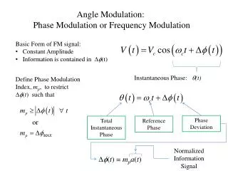
Modulation Formats General • The complete equation for an e – m wave can be substantially simplified if we limit • ourselves to modulation formats for high capacity transmission. Then, where β the propagation constant. In optics the symbol k is used instead of β so one should be aware of the implications in terminology. The equation above indicates that there are three parameters that can be used to impart information on the optical carrier. [1] Amplitude, E0; the format that modulates the amplitude of the optical carrier is called “amplitude modulation”. If the information is digital then the format is known as “ amplitude shift keying” or ASK for short. The format is also known in optical communications as “on off keying”, (OOK). In terms of the baseband signal the format is known as “non return to zero”, (NRZ). All these terms are used in the literature without restrictions. The basics of the ASK format is shown in the next slide for a NRZ baseband format.
1 Amplitude ≈ 0 Tb time Baseband signal Carrier Envelope 1 Amplitude ≈ 0 time ASK signal Modulation Formats General • [2] Frequency, ω; when the baseband signal modulates the frequency of the • optical carrier the process is called “frequency nodulation”. For digital baseband • signals it is called “ frequency shift keying”, (FSK). In the FSK format the • frequency of the carrier changes between “1” and “0”. The difference between • the two frequencies is not big but it is sufficient for the receiver to distinguish • the two frequencies and make the correct decisions. The ASK format with a binary NRZ baseband signal.
1 Amplitude ≈ 0 Tb time Baseband signal f0 carrier f1 carrier Constant envelope 1 Amplitude ≈ 0 time FSK signal Modulation Formats General • A typical FSK modulated signal is shown in the diagram below. The FSK format with a binary NRZ baseband signal with f0 < f1. Notice the contact envelope of the format in contrast to that of ASK where the short term power depends on the statistics of the baseband signal. This feature is helpful in designing the dynamic range of subsystems.
1 Amplitude ≈ 0 Tb time Baseband signal Phase 0 Phase π Constant envelope 1 Amplitude ≈ 0 time PSK signal Modulation Formats General • [3] Phase, θ; the modulation of the phase of the optical carrier is known as “phase • modulation”. For digital baseband signals is known as “phase shift keying”, • (PSK). In this format the phase of the carrier between “1” and “0” shifts by, say, • 180o. The actual details depend on the application. The PSK format for a binary • baseband signal is illustrated below. The PSK format with a binary NRZ baseband signal with the phase of “1” been 0 and the phase of “0” been shifted by π.
Modulation Formats General • The digital modulation formats were presented using a binary baseband signal. • However, each format can support multilevel signalling is necessary. For example, • A M-ary ASK signal has M -1 discrete “1” levels and the “0” level. Each pulse now • corresponds to As a result the M-ary signalling has been reduced to With M = 2 the baud rate equals the bit rate, Bb.
Complex plane Imaginary axis “1” (1, angle )V Real axis ● ● 0+ j 0 1+ j 0 “0” (0, angle 0)V (a) Conventional representation. (b) The “constellation” representation Modulation Formats The constellation concept • Until now the symbols of “1” and “0” for binary transmission have been defined as level • of, say, voltage or current. There is however an alternative representation that • conveys the same amount of information. Consider again a binary signal of “1” and “0” • and let us say that they correspond to voltages1 V and 0V that change with time. • Then, the complete description is one that contains also the phase, that is, phasors • are used for the complete description. The conventional representation is shown • below on the left. On the right there is the description using the complex plane. • Clearly, both representation contain the same about of information .The representation • on the right is called for reason that will become apparent very soon, the • “constellation”
Imaginary ● ● v2 01 Imaginary v1 00 ● ● ● ● v3 Real 10 Real ● ● v4 11 Modulation Formats The constellation concept • Perhaps, this example does not demonstrate the power of the new representation. • Consider now four voltages corresponding to four signal level represented by ; • v1=1+j 0, v2= 0+ j1, v3= -1+ j 0 and v4= 0 – j. The constellation is as shown below and • it should be clear now the advantages of the representation. In fact that constellation • represents a four level phase shift keying, (PSK), format. Now, let us farther assume • that the PSK four level format encodes bits according the following rule v1=00, • v2=01,v3=10 and v4=11. Then, instead of depicting the voltages the symbols can be • directly represented in the constellation diagram.
Amplitude – Random variable Amplitude 01 ● ● Phase 00 Phase – Random variable φ 01 00 ● ● 11 ● ● φ ● ● 10 11 Modulation Formats The constellation concept • The constellation diagram in the previous slide showed very clearly the position of the • symbols in the plane. In order to see the impact of transport consider the 4-symbol • PSK again but now rotated by 45o andusing the unit circle for reference. Notice, the • defined amplitude and phase of each symbol. This is the transmitted constellation. During transmission the constellation has been subjected to random amplitude and phase variations so the receiver has to estimate what was transmitted. See more on the use of signal constellation in assessing performance later.
Modulation Formats The spectral efficiency concept • Intuitively one expects that the available channel bandwidth is efficiently used to • transport information. This is achieved by using an efficient modulation format subject • to a number of constrains associated with system design. • Some definitions • [1] Bit rate; the bit rate defined the rate information is passed forward. • [2] Baud (or signalling) rate; defines the number of symbols per second. Each • symbol represents n bits, and has M signal states, where M = 2n. This is called • M-ary signalling. When n = 1, that is, one symbol is used to represents the • elements of the alphabet the signal has two states , M = 2. • Consider a simple example. A link can transport 50000 bit/s from A to B. The • bandwidth of the channel is 4000 Hertz. The spectral efficiency of the link, also • known as modulation efficiency, is 12.5 bit/s / Hz. • In spite of the similarity of definitions on spectral efficiency there are two variants that • are used; spectral efficiency in bits/Hz and modulation efficiency bits/baud.
Modulation Formats The spectral efficiency concept • Consider a system operating at 10 Gbit/s with channel spacing of 50 GHz. The • spectral efficiency is 10GBits / 50GHz = 0.2 bits/Hz. In this example the bits/baud is • 10GBits/10Gbauds = 1 bit/baud. The effective baud rate (symbol rate) is 10Gbauds.
Modulation Formats The Hartley – Shannon Law • The objective of any communication system is to transfer the maximum amount of • information with the minimum bandwidth. The famous Hartley – Shannon law • establishes an upper limit for reliable information transmission over a band limited • additive white Gaussian noise ,(AWGN), channel. The Hartley – Shannon law can be • stated as where C the channel capacity in bit/s, B the one sided channel bandwidth in Hz, S/N the signal to noise ratio, (SNR), but not in dB. If the SNR is given in dB it must be converted using the expression The information rate, R, must satisfy the equation
Modulation Formats The Hartley – Shannon Law • One useful variant of the Hartley – Shannon law is in terms of the average energy/bit, • Eb, (joules /bit) and the AWGN with two – sided noise spectral density N0/2. Then, • the signal power is S=Eb R and the noise power N=N0B and Now, Eb/N0 represent the SNR at the receiver in normalise form. The ratio R/B represents the spectral efficiency whose upper limits is C/B. The graph in the next slide illustrates the Harley – Shannon law. The curve corresponding to R = C separates the regions; below the line the spectral efficiencies are potentially achievable but above the curve they are unachievable. Clearly the question now is how do we calculate the [Eb/N0] (dB) for a given system? AS a simple example consider a 10 Gbit/s with an “on-off” NRZ format whose receiver has a sensitivity of - 20 dBm for 10-9 BER with detector responsivity R = 1.
Modulation Formats The Hartley – Shannon Law • Graph of the maximum achievable spectral efficiency [Bit/s/Hz ]as function of Eb/N0 (dB). R > C - Out of bounds area R = C Spectral efficiency (bit/s/Hz) 10 GBit/s example: BER=10-9 R < C – Accessible area R < C – Accessible area Eb/N0 (dB)
Modulation Formats The Hartley – Shannon Law • Step 1 We convert the power (-20 dBm) into the average optical power; thus Step 2 Assuming that the optical power is maximum for “1”, zero for “0” and a 50% probability of ”1” and “0” the peak optical power and energy/bit is Step 3 The value of N0-rms will be found from the BER. For a BER of 10-9 the ratio of peak optical power to rms noise is defined by the Q which is 12 for 10-9 BER.
Modulation Formats The Hartley – Shannon Law Step 4 The value of N0 will be foundby diving the N0-rms by the receiver bandwidth which for the sake of simplicity is 10 GHz; thus Step 5 The value of Eb/N0 is now Step 6 The spectral efficiency of the system is found by dividing the capacity by the bandwidth occupied by the spectrum ;since it is a NRZ format the effective spectral width is 20 GHz. Step 7 In the Hartley - Shannon graph the point for this system is at [8.0,0.5]. This point is plotted in the graph. Be aware that the derived noise spectral density was based on the BER.
Modulation Formats The Hartley – Shannon Law • There are two key features of spectral efficiency: • [1] Fundamental feature; higher signal-to-noise ratio is required for higher order • modulation. • [2] Practical feature; the implementation penalties are higher for higher • constellations and symbol rates.
Output pulses P1 Constant current source: Bias Constant current source: Modulator Imod Ibias Laser output Modulating signal Laser Ithr P0 Ibias I Isignal Input pulses Modulation Formats Intensity modulation • Historically, the first modulation format is intensity modulation. The reason for this is • the simple fact that semiconductor lasers are electrically pumped and they have very • short photon lifetimes. The circuit below is the basic circuit used for the intensity • modulation of semiconductor lasers. The diagram on the right shows the electronic and optical waveforms.
Modulation Formats Intensity modulation • In addition to a simple transmitter an intensity modulated optical carrier offers the use • of a very simple receiver for detection. All it requires is a p-i-n or apd detector followed • by a low noise electronic amplifier. This combination of intensity modulated carrier and • a p-i-n ( apd) receiver is referred to as “intensity modulated direct detection “,(IMDD), • system. Optical communications are used in a large number of diverse applications • and IMDD systems constitute the majority of systems used. • The simplicity of the direct intensity modulation of semiconductor lasers made possible • the introduction of optical fibre communications at an early date which required the • minimum of technical development. Hoverer, this simplicity brought a number of • issues such as; turn-on delay, relaxation oscillations, frequency response issues, • frequency chirping and unwanted frequency modulation. But continuous progress in • device design and material processing made possible to minimise these issues. • Directly modulated lasers cannot perform satisfactory for bit rates above 2.4 Gbits • because even with the up to date DFB lasers the impairments, especially dispersion, • reduce the performance to such an extent that cost effective systems cannot be • designed.
Modulation Formats Intensity modulation • Measured spectrum of a directly modulated laser under 622 MBit/s • NRZ modulation with 0.7 mW between ‘1’ and ‘0’ level.
Modulation Formats Intensity modulation Chirped spectrum; black. • Spectra calculated for the directly modulated laser under 622 MBit/s NRZ modulation. Theoretically expected spectrum; gray.
Modulation Formats Intensity modulation • The key issue here is that any attempt to directly modulate the laser impairs its • ability to function as a very high quality oscillator. • The solution to this problem is the use of external modulators. These are devices • modulate the optical radiation but they are external to the laser cavity and they do not • affect to the first order at least the dynamics of the cavity. The use of an external • modulator in addition to isolating the function of modulation from that of the • generation of very high quality optical radiation makes also possible to use modulation • schemes not supported by direct modulation.
v1(t) Waveguide Ein / 2 Ein Eout kEin / 2 Electrical Contacts v2(t) Modulation Formats Technology - Modulators • The discussion on modulation formats will be based on an external LiNbO3 modulator. • There are two reasons for this choice; firstly the devices and technology are mature • and deliver excellent performance and secondly it can deliver all the modulation • formats to be discussed. The basic outline of a amplitude travelling wave modulator is • shown below. The choice of a travelling wave modulator is dictated by bandwidth • requirements. The equation of the operation of an amplitude modulator also known as Mach-Zehnder (MZ) is given by,
Modulation Formats Technology - Modulators • With k = 1 the normalised output is written and with v1(t) = - v2(t) the phase term is removed and The details of the operation of a MZ amplitude modulator depend on the bias point of the device. In the next slide the power vs. input signal is shown. In the simplest application the device is biased at the point where the output power is half. This point is also known as the quadrature point. Then a drive peak-to-peak signal of Vπ is applied and the output swings between zero and full power. Different bias points enable the use of different modulation formats.
Power ● ● ● ● π 0 M - Z Modulator output Drive voltage 3Vπ Vπ 2Vπ 4Vπ Quadrature point Field Modulation Formats Technology - Modulators • One word of caution regarding the biasing point. Because of the material the bias point • drifts and careful design is necessary for ensuring the stability of the bias point. • One of the key features of modulation schemes is the bandwidth after modulation. The field and power output vs. drive voltage of a M - Z modulator.
Modulation Formats Technology - Modulators Left ; the basic modulator. • The architecture of a Mach – Zehnder modulator; from Photline Right ; the modulator with driver, terminating load and monitoring photodiode.
Frequency stabilised DFB laser Laser package Device fibre tail Transmission fibre TE element Optical isolator External modulator High quality optical connector Electronic amplifier Power to TE Temperature Bias current Power monitor Constant current bias source Laser TE Controller Data Modulation Formats Technology - Modulators • The architecture of an optical transmitter using an external modulator is, as expected, • more complex than that of a direct modulated one. The block diagram of a frequency • stabilised laser with a co-packaged external modulator is shown below.
Modulation Formats ASK signalling format • The ASK format is a very popular formats because of its simplicity and flexibility. • In some of the literature the term “on-off keying”, (OOK), is used instead. Starting with • a binary baseband signal one distinguishes two classes of ASK signalling: • [1] Non - return to zero format , (NRZ). • [2] Return to zero format, (RZ). • [1] Non – return to zero format; in this format the duration of the pulse (Tp) equals • the signalling interval (Tb) which is the inverse of the bit rate, Bb. A unity amplitude • NRZ pulse is shown below. A Tp -Tb/2 Tb/2 time Tb For a NRZ pulse the MZ is biased at quadrature and the input signal swings the modulator drive voltage between zero and Vπ.
Signal drive ● ● ● ● M -- Z power transmission Bias Phase 0 Phase π Vπ / 2 Vπ 2Vπ 3Vπ 4Vπ 0 Drive voltage Modulation Formats ASK signalling format The biasing and drive of a M-Z modulator for the NRZ format ASK format. Biasing the M-Z at the quadrature point and driving with a signal of Vπ amplitude the optical carrier swings between zero and the maximum value E0.
Modulation Formats ASK signalling format • One of the most important features of a carrier system is the bandwidth after • modulation. This feature is particular important in the context of WDM systems. For a • random binary stream of data in the baseband with equal probability for “1” and “0” • and with each pulse modelled as a rectangular pulse the baseband signal power • spectral density, (PSD), is given by the two sided function, The one sided PSD of this function is shown in the next slide with A = Tb = 1. Notice that the impulse at f = 0 carries half the power on the baseband signal and this is one of detrimental features of NRZ format because the power Is not used for information transmission.
Modulation Formats ASK signalling format • The PSD of the random unipolar signal for a NRZ rectangular pulse stream. PSD f
Modulation Formats ASK signalling format • When the baseband signal modulates the carrier the combined signal can be • represented as The two - sided PSD of the modulated carrier is now given by Since sinc2(f ± fc) = 0 the summation over k is zero. The one sided PSD of the ASK signal is shown in the next slide. The bandwidth after modulation is ≈ 2Bbase. This should not be a surprise because this a key feature of amplitude modulation in general.
Scarrier(f) Deterministic signal fc =optical carrier Bandwidth ≈ 2Bbase Stochastic signal fc f 90% of power 95% of power Modulation Formats ASK signalling format The PSD of a binary ASK signal in the optical domain.
Modulation Formats ASK signalling format • The modulation spectrum of a Mach – Zehnder modulator at 2.5 Gbit/s.
imaginary “1 to 0” threshold real ● ● “0” “1” ● ● “0 to 1” E0 State “0” State “1” Symbol “1” Symbol “0” Modulation Formats ASK signalling format • It is very instructive to construct the state and constellation diagram for the binary ASK • signalling format. State diagram Transition probabilities Constellation diagram for binary ASK signalling. State diagram and transition probabilities for binary ASK signalling.
Modulation Formats ASK signalling format • The PSD of a binary NRZ ASK signal for • 10 Gbit/s data without filtering. DC impulse Spectral nulls.
Modulation Formats ASK signalling format • The spectral of NRZ modulation at 10 and 40 Gbit/s. 10 Gbit/s. 40 Gbit/s.
A A A Tp Tp Tp time Tb time time Tb Tb Tp= 67% Tb Modulation Formats ASK signalling format • The key features of ASK signalling is that there is a DC term whose energy is not used • and it is difficult to recover timing information with long strings of “1” and “0”. The fact • that there will be long strings of “1” and “0” can be deduced from the state diagram of • NRZ format. Additionally, NRZ pulses are sensitive to the fibre dispersion. • [2] Return to zero format, (RZ); in this format the pulse width (Tp) is less than the • signalling interval ( Tb). Three typical RZ formats are shown below. Tp= 33% Tb Tp= 50% Tb
Modulation Formats ASK signalling format • The reasons for using RZ pulses are: • [1] High timing content. • [2] Reduced sensitivity to fibre dispersion. • However, these advantages are not without a price. The bandwidth of RZ pulses is • broader than that of NRZ and uses therefore more fibre bandwidth. This becomes an • issue in dense WDM,(DWDM), systems. In order to generate RZ optical pulses the • M - Z is biased at quadrature and the device is driven with a pulse of appropriate • width. For 50% duty cycle the M - Z is biased as per NRZ format. However, as the • pulse width is reduced it becomes progressively difficult to generates the narrow • pulses required. An alternative approach has been developed using two M - Z in • tandem and driven by different pulse streams. The concept is illustrated in the next • slide. The duty cycle of the output format depends on the bias and driving voltage of • the sinewave drive. Of course the transmitter is more complicated now but the • generation of RZ pulses with arbitrary duty cycle is much easier.
NRZ data Clock or sinusoid Data MZ Pulse carver MZ CW light Optical RZ format NRZ Modulation Formats ASK signalling format • In order to generate RZ50 pulses ( RZ pulse of 50% duty cycle) the pulse carver is • bias at quadrature and driven by a sinusoid of Vπ peak-to-peak voltage at the data • rate. The output pulses have an approximate 50% duty cycle and no additional phase • flipping. • A RZ33 pulseis created by driving the pulse carver with a 2Vπvoltage (peak to peak) • sinusoid at half the data rate, Bb/2, which is biased at the maximum of thetransfer • curve.Again, there is no phase flipping in the output. The concept of pulse carver modulator.
imaginary E0 real Tb / D ”0” “1” State ”1” State ”0” Symbol “0” Symbol “1” RZ67 D = 1.5 RZ50 D = 2 RZ33 D = 3 Modulation Formats ASK signalling format • RZ67 is created by driving the pulse carver with a 2Vπvoltage (peak to peak) sinusoid • at half the data rate, Br /2, which is biased at the null of the transfer curve. • The key effect of this type of pulse carving is that adjacent pulses always have • alternating zero and phase. In other words, the DC tone averages to zero since • alternating bits have opposite phase. As a result, the carrier is suppressed on average • and harmonic tones at +/- Br / 2 appear . The format is also known as Carrier • Suppressed RZ. The state diagram and the constellation for RZ formats is shown • below. The state diagram and the constellation for RZ formats.
RZ33 signal drive ● RZ50 signal drive RZ67 signal drive ● Bias M - Z power output Bias Phase 0 Phase π Bias ● 0 Vπ/2 Vπ 2Vπ 3Vπ 4Vπ M - Z voltage Modulation Formats ASK signalling format • The bias and drive requirements for generation of RZ pulses using the carver concept.
Modulation Formats ASK signalling format • The two sided PSD of RZ33 and RZ50 format is given by The pulses of various RZ formats.
Modulation Formats ASK signalling format • For RZ67 the PSD is given by The PSDs for RZ33, 50 and 67 from computer simulations are shown below. Modulation Formats Conversion for Future Optical Networks: Javier Cano Adalid MSc Thesis , TUD, 2009
Modulation Formats ASK signalling format • In order to understand how the carrier is suppressed with RZ67 one has to consider • the impact of phase. The optical pulses and their phase relationship is shown below. The sign of the carrier is changing at every bit transition and they are complete independent of the information carrying part of the signal. On average therefore The filed has a positive sign for half the ”1” bits and negative for the other half. This phase changes results in a zero mean optical field envelope. As a result the carrier at the optical centre frequency vanishes giving the format its name. Modulation Formats Conversion for Future Optical Networks: Javier Cano Adalid MSc Thesis , TUD, 2009