Acknowledgments:
Interfacing ultracold atoms with nanomagnetic. domain walls. A. D. West 1 , K. J. Weatherill 1 , T. Hayward 2 , D. Allwood 2 and I. G. Hughes 1 1 Joint Quantum Centre (JQC) Durham – Newcastle, Department of Physics, Durham University, Durham, DH1 3LE, UK

Acknowledgments:
E N D
Presentation Transcript
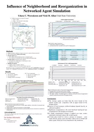
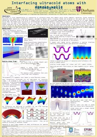
Interfacing ultracold atoms with nanomagnetic domain walls A. D. West1, K. J. Weatherill1, T. Hayward2, D. Allwood2 and I. G. Hughes1 1Joint Quantum Centre (JQC) Durham – Newcastle, Department of Physics, Durham University, Durham, DH1 3LE, UK 2Department of Engineering Materials, University of Sheffield, Sheffield, UK Abstract: We present a first demonstration of interaction of ultracold atoms with domain walls within magnetic nanowires. Planar permalloynanowires host oppositely orientated domains, divided by domain walls. Fringing fields are produced at the walls [1]. An array of serpentine nanowires gives a 2D array of domain walls, mimicing the sinusoidal magnetisation pattern required for an ideal magnetic mirror [2]. The domain wall structure is reconfigurable by external magnetic fields [3]. A cloud of ~107 87Rbatoms at 10 mK, optically pumped into the weak field seeking F=2, mF = 2 state is reflected by these fields. Monte Carlo simulations accurately predict the signal observed from an interrogating light sheet. Using the bounce signal we infer characteristics of the nanowire array. Future work aims to probe van der Waals potentials at short distances. We also present planned work to use the field from a single domain wall to create a tight (~1 MHz) atom trap. Once in such a trap, atoms can be transported above nanowires by application of a small magnetic field, inducing domain wall motion. Such a setup bears all the hallmarks of a scheme for quantum information processing. Magnetic Atom Mirror: Nanowires: • Made from Permalloy (Ni81Fe19) • Very soft ferromagnetic material • Negligible magnetocrystalline anisotropy • Lithographically fabricated using e-beam and lift off processing. An atom’s intrinsic magnetic moment, , interacts with field produced by nanowires: mFgF > 0 gives weak-field-seeking state; atoms entering fringing fields are repelled. Host head-to-head or tail-to-tail domain walls. Quasi-discontinuous magnetisation reversal (left) yields out of plane magnetic fields (bottom left) [1]. Ideal mirror has sinusoidal magnetisation, giving an evanescent field with a decay length proportional to the period of the pattern. A domain wall based mirror represents a quantum interface combining ultracold physics and spintronic technology. Domain Wall Array Periodic B Field Macroscopic shape determines the domain structure. Can image the resulting fringing fields using MOKE or scanning Hall probe microscopy (right). Field gradients up to 106 T/m. Choose a serpentine pattern of nanowires which produces a 2D array of domain walls. External fields toggle ‘on’ (lower) and ‘off’ (upper) states. Resulting periodic field mimics an ideal magnetic mirror (above right). We approximate the interaction as a point one, giving an effective surface (below right). Mobile Atom Trap: The field from a single domain wall can be approximated by [7]: Adding a bias field produces a trapping potential (left): Overview Experimental Setup The massive field gradients then give a very high trap frequency. The presence of a magnetic zero leads to rapid Majorana losses. Many conventional techniques are not applicable for nanoscale traps – we propose a new method of creating a time-averaged potential, using piezoelectric actuation [8]: We have observed the diffuse reflection of a cloud of ultracold atoms, shown in fluorescence images below [7]: Mechanical rotation of the field source produces a harmonic potential. The trap is also deeper and more adiabatic than conventional time-averaged potentials. We anticipate wTrap~MHz and depths of around 200 mK. R = 0.25 mm R = 0.50 mm R = 0.75 mm R = 1.00 mm We also use a weak light sheet to quantitatively analyse the dynamics. Results (left) are seen to agree well with Monte Carlo simulations. Colder atoms give a larger, better resolved signal. By increasing the amplitude of movement (R) the trap topology changes to being toroidal(above and below left). By reconfiguring the mirror we can tune the atom-nanowire interaction. The atoms then act as a probe of the micromagnetic reconfiguration (right). Results agree well with conventional magnetometry. The closest approach is very small (~50 nm) – enter van der Waals region. Traps based on domain walls are inherently mobile – they can be moved by currents or external fields. Networks of such traps present an ideal architecture for quantum information processing. References: [1] A. D. West, T. J. Hayward, K. J. Weatherill, T. Schrefl, D. A. Allwood and I. G. Hughes, A simple model for calculating magnetic nanowire domain wall fringing fields, J. Phys. D. 45, 095002 (2012). [2] E. A. Hinds and I. G. Hughes, Magnetic atom optics: mirrors, guides, traps and chips for atoms, J. Phys. D, 32 R119 (1999). [3] T. J. Hayward, A. D. West, K. J. Weatherill, P. J. Curran, P. W. Fry, P. M. Fundi, M. R. J. Gibbs, T. Schrefl, C. S. Adams, I. G. Hughes, S. J. Bending and D. A. Allwood, Design and characterization of a field-switchable nanomagnetic atom mirror, J. Appl. Phys. 108, 043906 (2010) [4] D. A. Allwood, T. Schrefl, G. Hrkac, I. G. Hughes and C. S. Adams, Mobile atom traps using magnetic nanowires, Appl. Phys. Lett. 89, 014102 (2006). [5] J. Fortágh and C. Zimmerman, Magnetic microtraps for ultracold atoms, Rev. Mod. Phys. 79 235 (2005) and references therein. [6] R. Folman, P. Krüger, J. Schmiedmayer, J. Denschlagand C. Henkel, Microscopic atom optics: from wires to an atom chip, Adv. Atom. Mol. Opt. Phys. 48 263 (2002) and references therein. [7] A. D. West, K. J. Weatherill, T. J. Hayward, P. W. Fry, T. Schrefl, M. R. J. Gibbs, C. S. Adams, D. A. Allwood and I. G. Hughes, Realization of the manipulation of ultracold atoms with a reconfigurable nanomagnetic system of domain walls, Nano Letters DOI: 10.1021/nl301491m. [8] A. D. West, C. G. Wade, K. J. Weatherilland I. G. Hughes, Piezoelectrically-actuated time-averaged atomic microtraps, Appl. Phys. Lett., 3 023115 (2012). Acknowledgments: This work was carried out in collaboration with colleagues at the University of Sheffield. This project is funded by EPSRC grants EP/F025459/1 and EP/F024886/1.