Download
1 / 25
250 likes | 372 Vues
Explore the design, features, and applications of the Timepix3 chip - a hybrid pixel detector offering high-resolution imaging capabilities. Learn about its evolution from Medipix1 to Medipix3, with a focus on functionalities like charge summing and energy resolution enhancement. The Timepix3 project aims to cater to various fields beyond high-energy physics, including X-ray imaging, dosimetry, and gamma polarization cameras. Delve into the technical aspects of readout chips for specific applications such as the LHCb VELO detector upgrade and micro-pattern gas detectors like GOSSIP and TPC. Discover the main features, block diagram, operation modes, and TDC architecture of Timepix3, showcasing its superior time resolution and energy efficiency.

E N D
Development and Applications of the Timepix3 chip Vladimir Gromov2 Christoph Brezina3, Martin van Beuzekom2, Michael Campbell 1, Klaus Desch3, Vladimir Gromov2, Xiaochao Fang3, Ruud Kluit 2, Andre Kruth3, Tuomas Poikela1,4, Xavi Llopart 1, Francesco Zappon2 ,Vladimir Zivkovic2 1CERN, Geneve, Switzerland, 2National Institute for Subatomic Physics (Nikhef), Amsterdam, the Netherlands 3Institute of Physics, Bonn University, Germany 4 University of Turku, Finland Vertex2011, Rust, Austria. June 24, 2011
Outline • Medipix / Timepix family of pixel detectors • Timepix3 : functionality and features • Design and performance of some basic circuits • Summary Vertex2011 V.Gromov 24/06/11 2
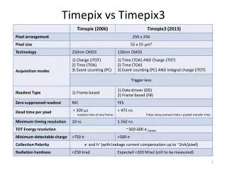
Medipix detectors • Photon (X-ray) counting hybrid pixel detector • Imaging / medical applications • 1997: Medipix1 (CERN) • - technology: 1μm CMOS • array: 64 x 64 • pixel: 170 um x 170 um • 2001-2005: Medipix2 (CERN) • - technology: 0.25μm CMOS, 6-metal • array: 256 x 256 • pixel: 55 um x 55 um • energy resolved photon counting • 2009: Medipix3 (CERN) • - technology: 0.13μm CMOS, 8-metal • array: 256 x 256 • pixel: 55 um x 55 um • charge summing mode • improved energy resolution Vertex2011 V.Gromov 24/06/11 3
Timepix pixel readout chip • TPC / micro-pattern gas detectors applications • measures hit arrival time OR energy deposit on each pixel • 2007: Timepix (CERN) • external clock : 100 MHz • full frame readout : serial port (10ms/frame) • Limitations • any event readout requires full frame • no zero suppression • dead time (no continuous readout) • time resolution is only 10ns (bin size) • slow front-end (time-walk ~120ns) Vertex2011 V.Gromov 24/06/11 4
Timepix3 project: design goals and current status • Timepix3 is an approved project of the Medipix3 collaboration with an assigned budget (2-engineering runs in 2012, 130nm CMOS) • wide range of non-HEP applications: • X-ray imaging • Dosimetry • Compton camera, gamma polarization camera, fast neutron camera, nuclear fission, astrophysics … • time-resolved imaging • hit (photon) → ToA & ToT • continuous & sparse readout • minimum dead time • suitable for HEP applications Vertex2011 V.Gromov 24/06/11 5
Required readout chips for the HEP applications • Upgrade of the LHCb VELO detector: VELOPIX • minimum pixel size • extremely high illumination: • up to 290 Mhits/cm2/s • continuous data readout • sparse data (zero suppression) • charge measurement • minimum pixel size • high time resolution: ~ 1ns • wide dynamic range : ~ 100μs • charge measurement • high sensitivity : threshold ≈ 350e- • Micro-pattern gas avalanche detectors: GOSSIP, TPC etc. Vertex2011 V.Gromov 24/06/11 6
Timepix3: main features Vertex2011 V.Gromov 24/06/11 7
Timepix3: top level block diagram 128 double-columns @ 256● 55μm = 1.4cm • pixel: 55μm x 55μm • Super Pixel: 8pixels @ 4 x 2 • 64 Super Pixels in a DC • 128 Double Columns (DC) • Super Pixel FIFO : 2-events • DC bus: 40MHz • End-of-DC FIFO: 4-events • Periphery bus: 40MHz @ 44b • Output Serializer / FIFO Analog Front-end Digital Region Readout Control (TOKEN based) Analog regions (30%) Time Stamp 14b ToT Counter 10b MUX DAC Double column bus Fast Counter 4b Digital region (70%) double column data bus (40MHz) Ring oscillator (640MHz) FIFO MUX Fast Counter 4b MUX ToT Counter 10b Time Stamp 14b DAC Data output block Serializer / FIFO 8-Pixel Region Tx FiFO periphery bus End of Column Logic Readout control (Token based) periphery data bus 40MHz Vcntr (oscillator) EFUSE chip ID Bandgap Bias gen. Slow control DAC Tx RX RX RX PLL Clock 8 x LVDS Data_out Data_in Reset_GLB Clock 40 MHz Vertex2011 V.Gromov 24/06/11 8
Timepix3: modes of operation Vertex2011 V.Gromov 24/06/11 9
High resolution TDC Shared Ring Oscillator architecture (per Super Pixel) Gated 640MHz CLK Hit_1 Counter_1 Pixel logic _1 SyncCLK Counter_2 Pixel logic _2 Counter_8 Pixel logic _8 Ring Oscillator Start / Stop 640MHz CLK OR Vcntr Time diagrams Preamp_out Hit SyncCLK (40MHz) Ring Oscillator Counter • low switching activity ~10-5 • negligible power consumption • compact design (~10% of the pixel area) Vertex2011 V.Gromov 24/06/11 10
RC Ring Oscillator NCAP = Varactor Vcntr VDD start / stop OUT NAND Control characteristic Effect of the power supply voltage • voltage-controlled • low sensitivity to the power supply • channel-to-channel mismatch ~1% Vertex2011 V.Gromov 24/06/11 11
TDC’s array with a PLL control DC_1 DC_2 DC_3 DC_4 Ring Oscillator • Features • immunity to variations • good uniformity • Gossipo-4 (Aug 8, 2011) Vcntr ∆V ≈ 0 Ring Oscillator Vcntr Icntr ≈ 0 Vcntr Ring Oscillator SyncCLK (40MHz) Charge Pump Loop Filter Phase Frequency Detector OUT Vcntr FbCLK (40MHz) :16 640MHz CLK Phase Locked Loop (PLL) Vertex2011 V.Gromov 24/06/11 12
Charge sensitive preamplifier • based on Krummenacher scheme • both input signal polarities (h+ and e-) Vdd=1.5V Ikrum Preamp_out signals -10 000e- electrons (e-) (Gas Detectors) source current -5 000e- Single-stage OPAMP -1 000e- Preamp_in Preamp_out 1 000e- 0.8V 5 000e- 0.36V Cd holes (h+) lpnfet Cfb=3fF 0.37V 10 000e- current sink Ck • high gain (50mV / 1ke-) • minimum time-walk (peaking time ~ 10ns) • low noise (σ ≈ 75e- @ Cd=25fF) • power 4.5μW (3μA @ 1.5V) Vertex2011 V.Gromov 24/06/11 13
Pulse height discriminator • threshold tuning per pixel (4bit) • fast response Time diagrams preamp output Preamp_out In1 Discr_out THR Vthr / polarity In2 discriminator output ∆t1 Threshold tuning (4bit) ∆t2 • power ≈ 6μW (4μA @ 1.5V) • internal delay ≈ 3ns • threshold mismatch ≈ 150e- • threshold mismatch (with tuning) ≈ 10e- Propagation delay 9 6 3 0 ∆t, ns discriminator output preamp output 0 -10k -20k -30k Qin, e- Vertex2011 V.Gromov 24/06/11 14
Readout of the chip Conventional readout link Embedded clock readout link Readout boards Readout boards Timepix 3 Timepix 3 Clock Clock Receive Engine Clock 8b /10b Encoding Clock Recovery block Data [0:7] Encoded signal {Clock + Data} Data Data Clock Data Encoded signal • 8b/10b encoding: 8b-word by 10b symbol • continuous activity for clock recovery • NO clock/data skew and synchronization issues • disparity correction (between 1’s and 0’s) • DC balance control • data alignment • data bus and clock bus are separate • synchronization loss at high rate Vertex2011 V.Gromov 24/06/11 15
Timepix3: interface part Periphery Data Bus: 44bit @ 40MHz DataIn Round-robin Distributor SyncCLK (40MHz) DataOut [0:7] 44bit Link is almost full Control Logic Slow control FIFO Mode of operation definition MUX 160MHz 320MHz 8bit Configuration data (threshold DAC’s, masks etc) 640MHz :10 Phase Locked Loop 8b/10b Encoder 10bit ½ Clock delay Clock_serial_link Serializer Data_serial_ link ReadoutCLK Ext. Readout clock SyncCLK (40MHz) Shutter Reset Busy Clock 1bit Data 1bit • Two modes of operation : • - encoded Clock – Data output (at 640 MHz) • - separate Clock and Data outputs (at 320MHz, 160MHz …. ) • selectable readout speed Vertex2011 V.Gromov 24/06/11 16
Summary • Timepix3 pixel readout chip is being developed in the frame of the Medipix3 collaboration for a wide range of applications • the chip is defined as a 256 by 256 pixel array (~2cm2) where each pixel measures 55μm by 55μm • for each hit both time-of-arrival will be measured with 1.6ns accuracy as well as charge deposit (time-over-threshold method) • the chosen architecture allows for continuous readout of the sparsely distributed data with the hit rate up to 20 ●106 cm-2 sec-1 • event count mode will also be available for imaging applications and for calibration • the chip is planned for submission in the beginning of 2012 Vertex2011 V.Gromov 24/06/11 17
Medipix-based detectors: the sensor Vertex2011 V.Gromov 24/06/11 19
Medipix family detectors • Photon (X-ray) counting hybrid pixel detector • Imaging / medical applications • 1997: Medipix1 (CERN) • - emerged from LHC1/Omega3 (technology: 1μm CMOS) • array: 64 x 64 / pixel: 170 um x 170 um / active area: 1.2cm2 • min detectable signal : 1 400 e- (5.1 keV in Si) • counter-per-pixel: 15-bit • shift register-based readout: 16b output bus @ 10 MHz (384μs) • 2001-2005: Medipix2 (CERN) • - technology: 0.25μm CMOS, 6-metal • array: 256 x 256 / pixel: 55 um x 55 um / active area: 2cm2 • energy window resolved photon counting: 2 discriminators • counter-per-pixel: 13-bit (14-bit) (max counting rate : 100kHz) • frame-based readout via: an LVDS TX: 1b @160MHz (< 9.2ms) • 32-bit parallel port (< 300us@100MHz) • 3-side buttable: chip interface at one side only • 2009: Medipix3 (CERN) • - technology: 0.13μm CMOS, 8-metal • array: 256 x 256 / pixel: 55 um x 55 um / active area: 2cm2 • highly configurable • improved energy resolution: charge summing mode • per pixel: 2 discriminators and 2 counters • continuous count-read mode : second counter is a storage buffer • designed for TSV (through-silicon via) Vertex2011 V.Gromov 24/06/11 20
Preamp: main specifications Vertex2011 V.Gromov 24/06/11 21
Charge deposit measurements: time-over-threshold method • wide dynamic range : ± 100 ke- Preamp_out signals Single-stage OPAMP Ikrum Preamp_out Preamp_in Qin -50 ke- I2 Cfb I1 Cd -25 ke- -10 ke- feedback - 5 ke- • Qin < 15ke- : input charge stored on Cfb • 15ke- <Qin < 100ke- : input charge stored on Cd • 100ke- < Qin : input charge is drained be the • parasitic diodes • discharge current is signal-dependent → • (INL ≈ 10% ) • channel-to-channel ToT mismatch ≈ 25% Preamp_in signals -25 ke- -50 ke- Vertex2011 V.Gromov 24/06/11 22
Accuracy of the ToT measurements • electronic noise causes time jitter: σjitter = σ(Uoutnoise) / [dU/dt] Preamp Output THR Comparator Output ToT= Qin / Idis σ(jitter) = σ(Uoutnoise) / [dU/dt] ↓ Idis/Cfb σ(jitter) / ToT = σ(Uoutnoise) ● Cfb / Qin time jitter • lowering of electronic noise • decreasing of the feedback capacitor Vertex2011 V.Gromov 20/06/11 23
Spartan-6 evaluation board (Peter Jansweijer) high-speed links Spantan-6 FPGA 3.2Gbps optical link supports links running at 640MHz Vertex2011 V.Gromov 24/06/11 24
Micro-pattern gas detectors: layout and features Gas-avalanche detector combining a gas layer as signal generator with a CMOS readout pixel array Cathode (drift) plane Cluster1 Cluster2 1mm …1m → Drift gap Cluster3 Gas Amplification Structure 400V 50um → Avalanche gap Readout chip Cpar Front-end circuit • - particle track image (projection) • 3D track reconstruction • no sensor leakage current compensation • low parasitic capacitance (less than 10fF) • - micro-discharges in avalanche gap TWEPP-09 V.Gromov 24/06/11 25