Download
1 / 34
350 likes | 374 Vues
Explore the process of vacuum brazing by Carlo Roncolato to achieve precise metal joining without excessive melting. Learn about brazing filler metals, technological aspects, and the benefits of this method.

E N D
Brazing, Copperplating,Vacuum Design C. Roncolato
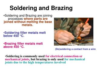
PhysicalIssues MainFeatures: • Brazing does not involve any substantial melting of the base metals • Maintain closer assembly tolerances and to produce a cosmetically neater joint without costly secondary operations. • Brazing makes it possible to join dissimilar metals (or metals to ceramics). Therefore, steel can be brazed to copper as easily as to another steel. • Brazing also generally produces less thermally induced distortion. An entire part can be brought up to the same brazing temperature. • Brazing readily lends itself to mass-production techniques. In fact, given the proper clearance conditions and heat, a brazed joint tends to make itself and is not dependent on operator skill, as are most fusion welding processes. • As a rule, the HAZ produced during brazing is wider and less sharply defined than those resulting from other fusion-related processes.
Brazing Filler Metal (BFM) Ternary Phase Diagram for Cu-Ag-Pd Three different alloys can be used to joint parts in several steps. The amount of Palladium determines the eutectic temperature and the joint performances.
TechnologicalIssues Water Connection Plug Base Water Channel Electrode Carlo Roncolato – INFN LNL +39 049 8068 477 – carlo.roncolato@lnl.infn.it
Welding Analysis The Brazing Filler Metal (BFM) is positioned in the grooves. After the melting for capillarity flows in the joint gaps, leaving a holes. Copper BFM BFM Voids Stainless Steel In red are shown some points for measurements Carlo Roncolato – INFN LNL +39 049 8068 477 – carlo.roncolato@lnl.infn.it
Eutethic Phase Formation Point 1 with 200x Point 1 with 830x This redistribution is accomplished by atomic diffusion. The microstructure of the solid that results from this transformation consists of alternating layers or zones of the Ag and Cu phases that form simultaneously during the transformation. This microstructure is called a eutectic structure. Carlo Roncolato – INFN LNL +39 049 8068 477 – carlo.roncolato@lnl.infn.it
EDAX Analysis It is possible to show where the chemical elements are positioned in the joints. Selective scanning are taken, while measuring a particular x-ray emission energy. Cu Fe Ag Ni Pd Cr Carlo Roncolato – INFN LNL +39 049 8068 477 – carlo.roncolato@lnl.infn.it
Effect of Cleaning Process BEFORE AFTER
PhysicalIssue Thickness Layer Material x3÷x4 skin depth = 30 mm Copper Electroplating 2÷4 nm Buffer Layer Nickel / Copper ≈ 50 mm Substrate Stainless Steel AISI 316L / Mild Steel r (resistivity) = 1.72 mW-cm
Experience at CERN (substrateis AISI 316L) 1/3 Small Parts UltrasonicDegreasing detergent NGL 17.40 spec. ALU III: 10 gm/lt temperature: 50 – 60°C time: 30 – 120 minutes frequency: 25 kHz Jet rinsing, followed by dipping in water. CathodicCleaning Detergent: Cleanor GL 301: 80 gm/lt Temperature: 30 - 35°C Voltage: 5 – 8 V, currentdensity: 5 – 7 A/dm2 Time: 30 – 60 s
Power Supply + − Experience at CERN (substrateis AISI 316L) 2/3 Small Parts Jet rinsing, followed by dipping in water. • Nickel Plating (Wood’s Bath) • Nickel Cloride: 300 gm/lt • Boric Acid : 30 gm/lt • Cloridric Acid : 50 ml/lt • Temperature: 50°C • Voltage: 1.5 – 3.5 V • CurrentDensity: 4 – 10 A/dm2 • Time: 1-2 min (pari a 3-5 mm) • AnodicEtching • Sulfuric acid 20% v/v • Temperature: Ambient (20°C) • Voltage: 5 – 6 V • Time: 10 – 15 sec. Jet rinsing, followed by dipping in water. • Activation • Cloridric Acid 50% v/v • Temperature: Ambient (20°C) • Time: 5 sec. No rinsing, afterwards! Nickel platingstrightaway Movement + − + Anode(Nickel) Sample (Cathode) Heater
Experience at CERN (substrateis AISI 316L) 2/3 Small Parts Jet rinsing, followed by dipping in water. • CopperPlating • CopperSulfate CuSO4 • 5 H2O: 75 g/l • Solforic Acid (conc.): 100 ml/l • Cloride: 0.075 g/l • Voltage: 1.5 – 3.5 V • Temperature: 20-30°C • CurrentDensity: 2 A/dm2 • Time: 75 minuti (pari a 30 mm) • Air blowing for mixing • Bath isfiltered
Experience at CERN (substrateis AISI 316L) 2/3 Small Parts Jet rinsing, followed by dipping in water and cathoderemoval • Deoxidize • Cloridric Acid 50% v/v • Temperature: Ambient (20°C) • Time: 10-20 sec. Jet rinsing, followed by dipping in water CopperPassivation Jet rinsing, followed by dipping in water Ultrasoniccleaning in demineralized water Rinsing with ethylalcoholfolloed by drying with nitrogen
Experience with Nichel Platingat LNL w/ «First» External company scratch test Scratch test parameters Type : Progressive BeginLoad (N) : 0 End Load (N) : 30 Loading rate (N/min) : 60 Speed (mm/min) : 13.62 Length (mm) : 7 AESensitivity : 5 Nickel Plating AISI 316LN
SEM Imagingafter scratch test. Head diameter 100mm Plastic deformation of the film with cracks
SEM Imagingafter scratch test. Head diameter 50mm Film isalreadycracked. Cracks are throughall the thickness The smaller head creates a deepergroove. Part of the films are removedgeneratingflakes.
Chemical Analysis with EDS a 20kV The Nickel platingseems to be contaminated with Zinc. Principio EDS Tempo acquisizione = 42s
Deposition from the «second» Company SEM Imagingafter scratch test. Head diameter 100mm
ThicknessCalibration 2.5mm 6.25 min/mm
Chemical Analysis with EDS 20 kV 12 kV
CoppertPlating Analysis (1/2) The actual thickness of the deposit on the plates were measured with a profile meter. The plates are masked in a way to have a “sharp” step between the Cu layer and the substrate. The interpolation shows the current density. J = 2.7 A/dm2 Carlo Roncolato – INFN LNL +39 049 8068 477 – carlo.roncolato@lnl.infn.it
CoppertPlating Analysis (2/2) EDS Principle Copperplating is free of other elements (1% range) Carlo Roncolato – INFN LNL +39 049 8068 477 – carlo.roncolato@lnl.infn.it
Scratch Test & SEM analysis Micro Scratch Test with head of 100μm
Scratch Test & SEM analysis Micro Scratch Test with head of 50μm
ElectroplatingRecipe Buffer layeris made of copper
Problem with plating Solution? Solution? Choose a proper Curvature Radius Reversing
RFQ tank for SPES • Mechanical Specifications: • no. 6 tanks • FInt= 754 mm • Length ≈1150 mm • Weight 990 kg (approx) • General Requirements: • Operating Pressure< 1x10⁻⁸mbar • Cleanliness from dustparticles and oil • Limited Vibration • No Maintenance