Download
1 / 40
450 likes | 1.25k Vues
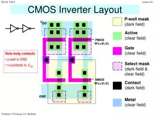
Inverter Circuit Layout DRC & LVS. Integrated Circuit Application and Design Lab. Chung Yuan Christian University Prepared by C. Y. Chiou. Inverter Layout Step 1. i >> NMOS_Mn1 F3 >> PMOS_Mp1 將兩條 POLY 對齊. Inverter Layout Step 2. 連接 PMOS 與 NMOS 的 Drain 端. Inverter Layout Step 3.

E N D
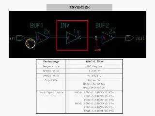
Inverter Circuit LayoutDRC & LVS Integrated Circuit Application and Design Lab. Chung Yuan Christian University Prepared by C. Y. Chiou
Inverter Layout Step 1 • i >> NMOS_Mn1 • F3 >> PMOS_Mp1 • 將兩條POLY對齊
Inverter Layout Step 2 • 連接PMOS與NMOS 的Drain端
Inverter Layout Step 3 • 將MCO(旋轉90度)放置於PMOS與NMOS中間,並使其右方貼齊POLY
Inverter Layout Step 4 • 觀察MCP上的Metal 1與另一條Metal 1之距離,發現其間距為0.195, 而M1.S.1=0.23
Inverter Layout Step 5 • 為符合Design Rule,將其間距修改為0.23,亦即將MCP往左移0.035
Inverter Layout Step 6 • 觀察圖中之POLY與P-IMP之距離,發現間距為-0.33,而PO.C.1=0.1
Inverter Layout Step 7 • 為符合Design Rule,將其間距修改為0.1,亦即將MCP往下移0.43
Inverter Layout Step 8.1 • 由於此時是採用Hierarchy的方式來作Layout,故Layout Editor無法偵測到Cell內部的DIFF. • 為能夠使用Layer Generation的功能來產生N-Well,故此時另外在PMOS的DIFF上畫一個相同的DIFF. • 畫完DIFF之後,利用Ctrl+f來確認.
Inverter Layout Step 8.2 • 待確認完後,用Shift+f切換回來
Inverter Layout Step 9.1 • 1. 圈選剛才畫的DIFF • 2. Create >> Layer Generation • 3. OK OD.C.4 = 0.43
Inverter Layout Step 10 • 在PMOS上方採用DIFF任意畫一個矩型,使其寬度和PMOS的DIFF相同. • 矩形長度 = 0.48*2+0.18 = 1.14 • (1.14-0.42)/0.47=1.53... • 1.14-(0.42+0.47)=0.25 • 0.25/2=0.125
Inverter Layout Step 11.1 • 1. i >> MCO (Rotate) >> Columns =2, Delta X=0.47 >> OK • 2. 將MCO擺放在DIFF中央,並貼齊矩形. 如圖中距離左方為0.125,距離右方為0.125 • 3. 調整DIFF之高度,使其和MCO等高
Inverter Layout Step 12.1 • 1. 點選剛才畫的DIFF • 2. Create >> Layer Generation • 3. OK • 4. 觀察P-IMP和N-IMP之距離(PMOS) NP.C.1=0.26
Inverter Layout Step 12.2 • 距離為0 • NP.C.1=0.26 • 必須將整個Substrate上移0.26
Inverter Layout Step 13.1 • 1. 觀察N-IMP Buttom之Y座標,圖中為8.395
Inverter Layout Step 13.2 • 2. m; 3.圈選整個Substrate; 4. F3
Inverter Layout Step 13.3 • 4. 將Y改為0.26 >> Apply XY >> Hide
Inverter Layout Step 14.1 • 觀察N-IMP之TOP與 N-Well之TOP的間距 • 距離為(-0.96) • OD.C.1=0.12 • 必須將整個N-Well延伸0.96+0.12=1.08
Inverter Layout Step 14.2 • 觀察N-Well TOP之Y座標,圖中為8.475
Inverter Layout Step 14.3 • 點選N-Well • q • 將Top改為9.555(=8.475+1.08) • OK • f
Inverter Layout Step 15.1 • 觀察N-Well 之Buttom與 N-IMP之TOP的間距 • 距離為(-0.34) • OD.C.2=0.43 • 必須將整個N-MOS往下移動0.34+0.43=0.77
Inverter Layout Step 15.2 • 1. m; • 2. 點選整個NMOS; • 3. F3 • 4. 將Y的部份改為-0.77 • 5. Apply XY • 6. OK
Inverter Layout Step 15.3 • 觀察圖中之POLY與N-IMP之距離, 發現間距為-0.01,而PO.C.1=0.1
Inverter Layout Step 15.4 • 1. m; • 2. 點選整個NMOS; • 3. F3 • 4. 將Y的部份改為-0.11 • 5. Apply XY • 6. OK
Inverter Layout Step 16 • c • 圈選整個Substrate (PMOS) • 複製至NMOS下方
Inverter Layout Step 17.1 • 點選N-IMP • q • 將Layer改為PIMP • OK (不要按Apply,否則會產生2層不同的Layer)
Inverter Layout Step 17.2 • 觀察N-MOS 之P-IMP與 N-IMP之TOP的間距 • 距離為0.16 • PP.C.1=0.26 • 必須將整個Substrate往下移動0.26-0.16=0.1
Inverter Layout Step 17.3 • 1. m; • 2. 圈選整個Substrate; • 3. F3 • 4. 將Y的部份改為(-0.1) • 5. Apply XY • 6. OK
Inverter Layout Step 18.1 • 連接PMOS的Source和Substrate
Inverter Layout Step 18.2 • 填滿PMOS的Substrate內部MCO之間的空隙
Inverter Layout Step 18.3 • 連接NMOS的Source和Substrate
Inverter Layout Step 18.4 • 填滿NMOS的Substrate內部MCO之間的空隙
Inverter Layout Step 18.5 • 連接NMOS和PMOS的Drain端
Inverter Layout Step 18.6 • 連接NMOS和PMOS的Gate端
Inverter Layout Step 19 Fix DRC Error: M1.A.1 0.23*0.34=0.0782 0.202/0.23=0.8783…<0.88