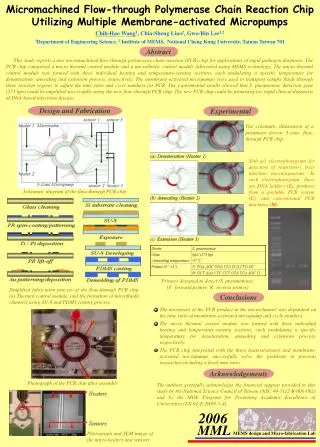
Micro-fabrication
Micro-fabrication. Photolithography-Outline. History Methods and Theories of Photolithography Preparation and Priming Spin-Coating Photoresists Soft-baking Mask Alignment and Exposure Developing Hard-baking. History.

Micro-fabrication
E N D
Presentation Transcript
Photolithography-Outline • History • Methods and Theories of Photolithography • Preparation and Priming • Spin-Coating • Photoresists • Soft-baking • Mask Alignment and Exposure • Developing • Hard-baking
History • Historically, lithography is a type of printing technology that is based on the chemical repellence of oil and water. • Photo-litho-graphy: latin: light-stone-writing • In 1826, Joseph Nicephore Niepce, in Chalon, France, takes the first photograph using bitumen of Judea on a pewter plate, developed using oil of lavender and mineral spirits • In 1935 Louis Minsk of Eastman Kodak developed the first negative photoresist • In 1940 Otto Suess developed the first positive photoresist. • In 1954, Louis Plambeck, Jr., of Du Pont, develops the Dycryl polymeric letterpress plate
Photolithography • In photolithography, the pattern is created photographically on a substrate (silicon wafer) • Photolithography is a binary pattern transfer: there is no gray-scale, color, nor depth to the image • This pattern can be used as a resist to substrate etchant, or a mold, and other forms of design processes • The steps involved are wafer cleaning, photoresist application, soft baking, mask alignment, and exposure and development
Preparation and Priming • Prepare the substrate : • Wash with appropriate solvent to remove any matter and other impurities • TCE, Acetone, MeOH • Dry in Oven at 150°C for 10 min. • Place on hotplate and cover with petri dish, let temp. stabilize at 115°C. • Deposit Primer (optional) • Chemical that coats the substrate and allows for better adhesion of the resist TCE = trichloroethylene, MeOH = methanol
Spin-Coating the Resist • Spin on the photoresist to the suface of the wafer • Standard methods are to use high spin coaters • rpm: • Time: • Produces a thin uniform layer of photoresist on the wafer surface. • Exposure Use UV light at this stage
Photoresist • Photoresist is an organic polymer which changes its chemical structure when exposed to ultraviolet (UV) light. • It contains a light-sensitive substance whose properties allow image transfer onto a printed circuit board. • There are two types of photoresist: positive and negative
Diagram: • Exposure to UV light causes the resist to polymerize, and thus be more difficult to dissolve • Developer removes the unexposed resist • This is like a photographic negative of the pattern • Exposure to UV light makes it more soluble in the developer • Exposed resist is washed away by developer so that the unexposed substrate remains • Results in an exact copy of the original design
Soft-Baking • Put on hotplate, or in oven • Temperature;Time • Removes volatile solvents from the coating • Makes photoresist non-sticky • Hardens to amorphous solid • Be careful not to over bake and destroy the sensitizer
Mask Alignment and Exposure • Photomask is a square glass plate with a patterned emulsion of metal film on one side • After alignment, the photoresist is exposed to UV light • Three primary exposure methods: contact, proximity, and projection
Photoresist Developer • Highly-pure buffered alkaline solution • Removes proper layer of photoresist upon contact or immersion • Degree of exposure affects the resolution curves of the resist
Hard Baking • Final step in the photolithographic process • Not always necessary; depends on the resist • Hardens the photoresist • Improves adhesion of the photoresist to the wafer surface
Etching • Etching type Wet etching Dry etching • Etching steps Oxidation Reaction Remove products
Factors in Wet Etching • Limited • • Reaction limited • • Diffusion limited • • Factors • • Concentration • • Temperature • • Stirring
HNA • mixture of nitric (HNO3), hydrofluoric (HF) and acetic (CH3COOH) acids • HNO3 oxides Si, HF removes SiO2, repeat… • high HNO3:HF ratio (etch limited by oxide removal) • low HNO3:HF ratio (etch limited by oxide formation) • dilute with water or acetic acid (CH3COOH) • acetic acid is preferred because it prevents HNO3 dissociation